Raevenlord
News Editor
- Joined
- Aug 12, 2016
- Messages
- 3,755 (1.20/day)
- Location
- Portugal
| System Name | The Ryzening |
|---|---|
| Processor | AMD Ryzen 9 5900X |
| Motherboard | MSI X570 MAG TOMAHAWK |
| Cooling | Lian Li Galahad 360mm AIO |
| Memory | 32 GB G.Skill Trident Z F4-3733 (4x 8 GB) |
| Video Card(s) | Gigabyte RTX 3070 Ti |
| Storage | Boot: Transcend MTE220S 2TB, Kintson A2000 1TB, Seagate Firewolf Pro 14 TB |
| Display(s) | Acer Nitro VG270UP (1440p 144 Hz IPS) |
| Case | Lian Li O11DX Dynamic White |
| Audio Device(s) | iFi Audio Zen DAC |
| Power Supply | Seasonic Focus+ 750 W |
| Mouse | Cooler Master Masterkeys Lite L |
| Keyboard | Cooler Master Masterkeys Lite L |
| Software | Windows 10 x64 |
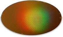
The possibility barely exists to account for all the silicon manufacturing processes currently in development; TSMC themselves are rolling out 5 nm, 4 nm, 3 nm, and 2 nm processes at various points in time in the future. Now, the company has announced that it will be rolling out a revision of the 3 nm manufacturing process, named 3 nm Plus, come 2023. According to DigiTimes, the Taiwanese manufacturer's first client for this process will be Apple.
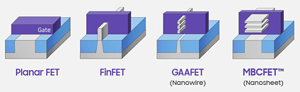
There is no information on what exactly 3 nm Plus leverages and offers over the "vanilla" 3 nm process. It could be anything from higher transistor density, lower power consumption, or higher operating frequency - or maybe a mixture of the three. The original 3 nm manufacturing process is set to offer a 15% performance gain over the current top-of-the-line 5 nm node, with 30% decreased power use and up to 70% density increase. Interestingly, TSMC is keeping their FinFet manufacturing technology, on grounds of better implementation costs and higher power efficiency compared to the more exotic GAA (Gate-All-Around) technology that its rival Samsung, for one, aims to implement in 3 nm.

View at TechPowerUp Main Site
There is no information on what exactly 3 nm Plus leverages and offers over the "vanilla" 3 nm process. It could be anything from higher transistor density, lower power consumption, or higher operating frequency - or maybe a mixture of the three. The original 3 nm manufacturing process is set to offer a 15% performance gain over the current top-of-the-line 5 nm node, with 30% decreased power use and up to 70% density increase. Interestingly, TSMC is keeping their FinFet manufacturing technology, on grounds of better implementation costs and higher power efficiency compared to the more exotic GAA (Gate-All-Around) technology that its rival Samsung, for one, aims to implement in 3 nm.


View at TechPowerUp Main Site


")


