While I agree in principle, and I definitely want a higher CU count APU ASAP, given that these are quite large monolithic dice made on a cutting-edge node it's kind of understandable that it hasn't happened yet. And I don't think it will for a while, sadly.
Renoir is reasonably large at
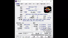
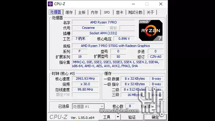
~149mm2 (~11*13.6mm). Now, the aspect ratios from the Videocardz die shot above and AnandTech's measurements don't quite line up (the VC shot is a bit less than 0.75:1 while 11*13.6 is 0.81:1), so these numbers will be a bit off. Still, Cezanne has a more square (but not quite) aspect ratio - assuming a similar error as for Renoir and that the die width is the same (which it looks like) let's say it's 13,6mm square for the sake of simplicity. That's 185mm2. That relatively small increase in die size means a drop in dice per wafer from 381 to 304 (20%) and likely defect-free dice from 333 to 258 (22,5%), assuming the same process and yields (with TSMC's published 0.09/cm2 error rate). So just by going from Zen 2 to Zen 3 we're increasing per-die costs by >20%. Using some slightly oversimplified math (defective dice are still utilized as much as possible after all), assuming a ~$20 000 cost per wafer that's an increase in per-die cost from ~$60 to ~$77.5 Adding even a couple more CUs would further increase costs, possibly bringing per-die costs close to the $100 range.
Now, this would be reasonable for a premium, high-performance part. The issue is that these are mass-market parts used in the entire spectrum of APUs from AMD. This also at least partially explains the continued use of the Lucienne Zen 2 SKUs in the mobile APU lineup, btw, as they will still perform well (and have power efficiency updates since Renoir) but are significantly cheaper and easier to produce in higher volumes. But that's besides the point.
The issue here is that AMD is using a single monolithic die to create everything from high-end mobile APUs (35-45W Ryzen 7/9 5xxxH) to desktop APUs (65W Ryzen 7/9 5xxxG) to mid-range thin-and-light chips like the 15W 5600U. They've excluded these more expensive chips from the very low end by using Lucienne there (and I guess also the rumored Van Gogh for lower-power implementations, though it's so far nowhere to be seen, and rumored to have been cancelled due to fab constraints). That's a pretty large range, and it inevitably means a cost squeeze for the lower end parts. Raising per-die production costs makes that squeeze harder - and lower end SKUs sell in much higher volumes than higher end ones, after all. the Ryzen 5 5600U is likely to outsell the Ryzen 7 5800H by 10:1 or more, so it's imperative that they make some money even on the low end SKUs.
This dilemma can be solved one of two ways: by making more monolithic dice (which AMD is sort of sliding into, though not through concurrently designing several variants of the same silicon like Intel, but rather by iterating on older designs while introducing newer ones), or by implementing a chiplet approach for APUs too. The former, if continued to the point that they need to concurrently design 2-3 APU dice each generation, is really expensive. The latter is, so far, seemingly too complex. This might be down to substrate-based IF links being too power hungry, issues packaging and cooling direct-die MCM laptop chips, package size constraints (MCM needs more area than monolithic dice), a combination thereof, or anything else, really. I still think we'll see MCM APUs in the future, but I think until then, we won't see a proper high-performance iGPU APU like us enthusiasts seem to want - it's simply too expensive, and doesn't make sense economically in the grand scheme of chip production.
I'm hoping that AMD is planning to get MCM APUs into the market alongside mainstream (LP)DDR5 adoption in laptops. That would be pretty much perfect. But IMO that's a pretty optimistic vision.