- Joined
- Aug 19, 2017
- Messages
- 2,811 (1.02/day)
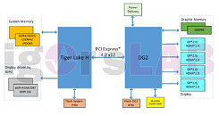
Yesterday, we got information that Intel's upcoming DG2 discrete graphics card is "right around the corner". That means that we are inching closer to the launch of Intel's discrete GPU offerings, and we are going to get another major player in the current GPU market duopoly. Today, however, we are in luck because Igor from Igor's LAB has managed to get ahold of the specifications of Intel's Xe-HPG DG2 graphics card. For starters, it is important to note that DG2 GPU will first come to laptops later this year. More precisely, laptops powered by Alder Lake-P processors will get paired with DG2 discrete GPU in the second half of 2021. The CPU and GPU will connect using the PCIe 4.0 x12 link as shown in the diagram below, where the GPU is paired with the Tiger Lake-H processor. The GPU has its subsystem that handles the IO as well.

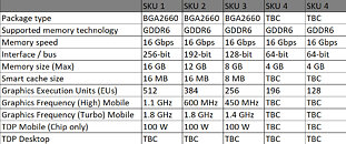
Next up, we have the specifications of various SKUs. Intel has prepared as many as five SKUs, each differentiating in Execution Unit (EU) count and memory interface configuration. Starting with the biggest model, the 512 EU, 4096 core design, this SKU will be DG2's biggest model. It will feature 16 GB of GDDR6 VRAM, running at 16 Gbps speeds on a 256-bit memory bus. It has 16 MB of so-called smart cache present inside the GPU. While the desktop variant clock speeds and TGP are unknown, the base clock of mobile design is 1.1 GHz, with a boost speed of 1.8 GHz. The TGP of this GPU is rated at 100 Watts, which is the average for higher-end GPUs in laptops. This SKUs smaller brother is a design with 384 EUs and 3072 cores, up to 12 GB of GDDR6 VRAM on a 192-bit memory bus. This one has a base clock of just 600 MHz, while the boost speed goes up to 1.8 GHz. You can find the rest of the specifications in the table below, as well as to check out other SKUs.
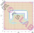
Additionally, Igor's LAB got ahold of the PCB diagram that shows the board layout of DG2 in the laptop along with the CPU. The DG2 GPU is seated on the BGA2660 socket, which is also pictured below with the pin configuration.

View at TechPowerUp Main Site


Next up, we have the specifications of various SKUs. Intel has prepared as many as five SKUs, each differentiating in Execution Unit (EU) count and memory interface configuration. Starting with the biggest model, the 512 EU, 4096 core design, this SKU will be DG2's biggest model. It will feature 16 GB of GDDR6 VRAM, running at 16 Gbps speeds on a 256-bit memory bus. It has 16 MB of so-called smart cache present inside the GPU. While the desktop variant clock speeds and TGP are unknown, the base clock of mobile design is 1.1 GHz, with a boost speed of 1.8 GHz. The TGP of this GPU is rated at 100 Watts, which is the average for higher-end GPUs in laptops. This SKUs smaller brother is a design with 384 EUs and 3072 cores, up to 12 GB of GDDR6 VRAM on a 192-bit memory bus. This one has a base clock of just 600 MHz, while the boost speed goes up to 1.8 GHz. You can find the rest of the specifications in the table below, as well as to check out other SKUs.

Additionally, Igor's LAB got ahold of the PCB diagram that shows the board layout of DG2 in the laptop along with the CPU. The DG2 GPU is seated on the BGA2660 socket, which is also pictured below with the pin configuration.


View at TechPowerUp Main Site


