- Joined
- Oct 9, 2007
- Messages
- 47,538 (7.47/day)
- Location
- Hyderabad, India
| System Name | RBMK-1000 |
|---|---|
| Processor | AMD Ryzen 7 5700G |
| Motherboard | ASUS ROG Strix B450-E Gaming |
| Cooling | DeepCool Gammax L240 V2 |
| Memory | 2x 8GB G.Skill Sniper X |
| Video Card(s) | Palit GeForce RTX 2080 SUPER GameRock |
| Storage | Western Digital Black NVMe 512GB |
| Display(s) | BenQ 1440p 60 Hz 27-inch |
| Case | Corsair Carbide 100R |
| Audio Device(s) | ASUS SupremeFX S1220A |
| Power Supply | Cooler Master MWE Gold 650W |
| Mouse | ASUS ROG Strix Impact |
| Keyboard | Gamdias Hermes E2 |
| Software | Windows 11 Pro |
Senior Technology Fellow Yuzo Fukuzaki shed light on the elusive new CPU technology AMD unveiled at its Computex 2021 keynote, 3D Vertical Cache (3DV Cache). The company had then detailed it as an additional 64 MB last-level cache stacked on top of a CCD (CPU core complex die), which significantly improves performance, including a claimed 15% average gain in gaming performance, which accounts for a generational performance gain over "Zen 3." The prototype AMD unveiled in its keynote was based on a Socket AM4 processor with "Zen 3" CCDs that have the 3DV Cache components in place. With two such CCDs, a 16-core processor would end up with 192 MB of L3 cache.
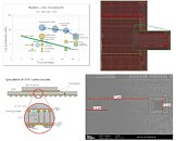
Yuzo Fukuzaki's theory sheds light on the most plausible position of 3DV Cache in the processor's cache hierarchy. Apparently, it expands the CCD's L3 cache, and doesn't serve as an "L4" victim cache to the L3. This way, the cache setup remains transparent to the OS, which sees it as a contiguous 96 MB block of L3 cache (per CCD). The 3DV Cache die is an SRAM chip fabricated on the same 7 nm process as the "Zen 3" CCD. It measures 6 mm x 6 mm (36 mm²), and is located above the region of the CCD that typically has the 32 MB L3 SRAM. Fukuzaki estimates that roughly 23,000 TSVs (through-silicon vias), each about 17 µm in size, connect the 3DV Cache die to the main CCD.

View at TechPowerUp Main Site
Yuzo Fukuzaki's theory sheds light on the most plausible position of 3DV Cache in the processor's cache hierarchy. Apparently, it expands the CCD's L3 cache, and doesn't serve as an "L4" victim cache to the L3. This way, the cache setup remains transparent to the OS, which sees it as a contiguous 96 MB block of L3 cache (per CCD). The 3DV Cache die is an SRAM chip fabricated on the same 7 nm process as the "Zen 3" CCD. It measures 6 mm x 6 mm (36 mm²), and is located above the region of the CCD that typically has the 32 MB L3 SRAM. Fukuzaki estimates that roughly 23,000 TSVs (through-silicon vias), each about 17 µm in size, connect the 3DV Cache die to the main CCD.

View at TechPowerUp Main Site


