- Joined
- Oct 9, 2007
- Messages
- 47,878 (7.38/day)
- Location
- Dublin, Ireland
| System Name | RBMK-1000 |
|---|---|
| Processor | AMD Ryzen 7 5700G |
| Motherboard | Gigabyte B550 AORUS Elite V2 |
| Cooling | DeepCool Gammax L240 V2 |
| Memory | 2x 16GB DDR4-3200 |
| Video Card(s) | Galax RTX 4070 Ti EX |
| Storage | Samsung 990 1TB |
| Display(s) | BenQ 1440p 60 Hz 27-inch |
| Case | Corsair Carbide 100R |
| Audio Device(s) | ASUS SupremeFX S1220A |
| Power Supply | Cooler Master MWE Gold 650W |
| Mouse | ASUS ROG Strix Impact |
| Keyboard | Gamdias Hermes E2 |
| Software | Windows 11 Pro |
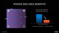
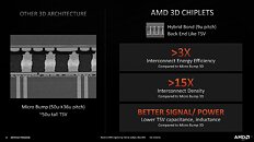
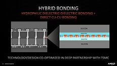
AMD in its HotChips 33 presentation shed light on the the company's efforts to stay on the cutting edge of 3D silicon packaging technology, especially as rival Intel takes giant strides with 2.5D and 3D packaging on its latest "Ponte Vecchio" and "Sapphire Rapids" packages. The company revealed that it co-developed a pioneering new die-on-die stacking technique with TSMC for its upcoming "Zen 3" CCDs with 3D Vertical Caches, which are 64 MB SRAM dies stacked on top of "Zen 3" CCDs to serve as an extension of the 32 MB on-die L3 cache. The micro-bumps connecting the 3D Vertical Cache die with the CCD are 9-micron in pitch, compared to 10-micron on the production variant of Intel Foveros.
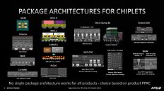
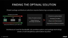
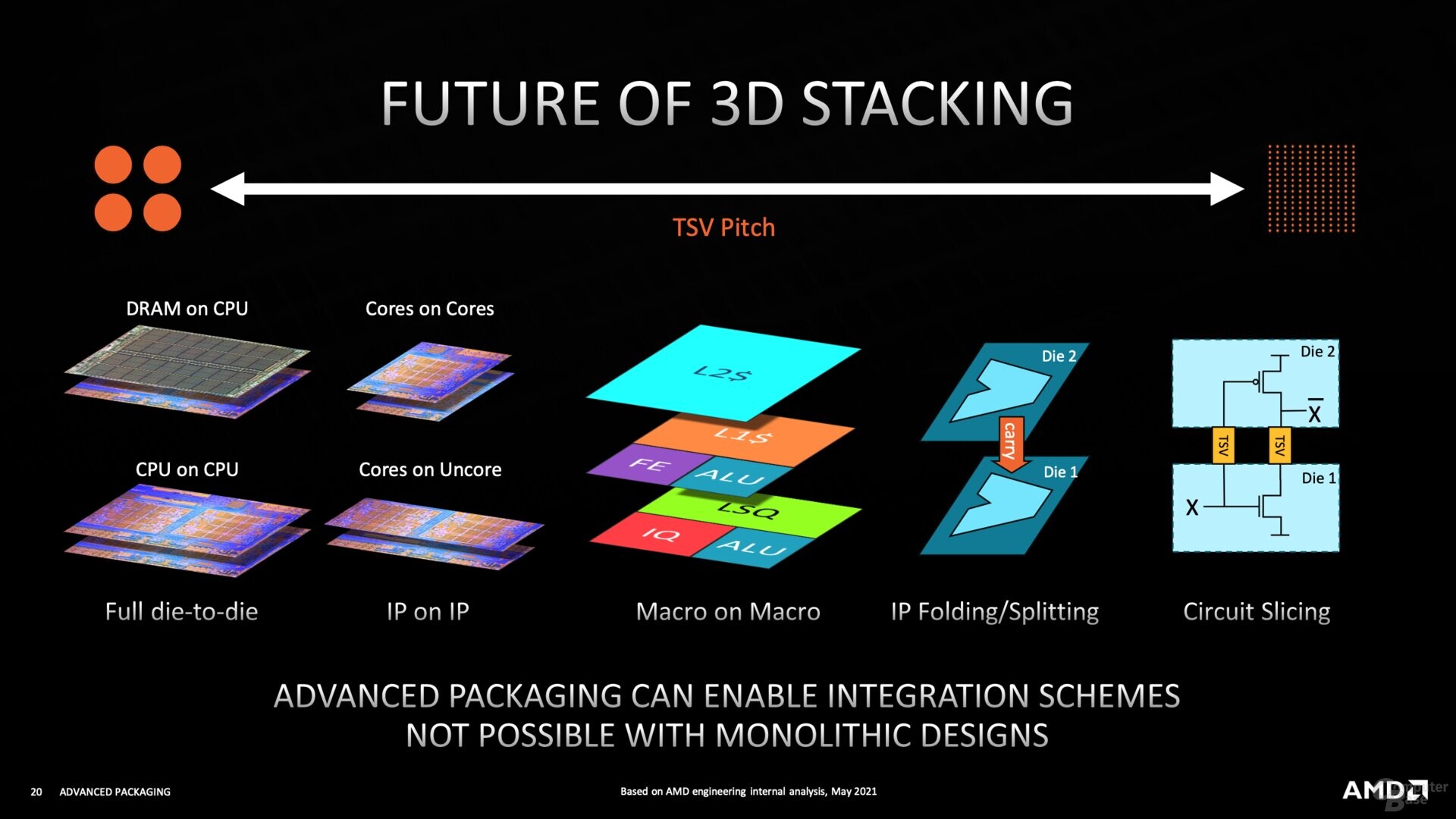
AMD believes that no single packaging technology works for all products, and depend entirely on what it is you're trying to stack. The company spoke on the future of die-on-die stacking. For over a decade, package-on-package stacking has been possible (as in the case of smartphones. Currently, it's possible to put memory-on-logic within a single package, between the logic die and an SRAM die for additional cache memory; a logic die an DRAM for RAM integrated with package; or even logic with NAND flash for extreme-density server devices.

The future could see IP-on-IP dual-logic stacking. Examples of this include cores-on-uncore, or even core-on-core. Imagine stacking the CCDs directly on top of the cIOD or sIOD dies to minimize the PCB footprint of the package; or the holy grail of 3D: stacking cores on top of cores.
A level beyond this would be splitting up the core itself into bits, and stacking them up. This could see the hottest components, such as the execution stage with its FP and INT pipelines on a different die than the relatively cooler front-end and load-store units; while the relatively coolest L1 and L2 caches, sit on the lowest slices.
The distant future of silicon stacking sees individual circuits spread across multiple stacked dies, with TSVs (through-silicon vias) connecting them. With each generation shift, AMD expects TSV sizes (and densities) to increase.
View at TechPowerUp Main Site
AMD believes that no single packaging technology works for all products, and depend entirely on what it is you're trying to stack. The company spoke on the future of die-on-die stacking. For over a decade, package-on-package stacking has been possible (as in the case of smartphones. Currently, it's possible to put memory-on-logic within a single package, between the logic die and an SRAM die for additional cache memory; a logic die an DRAM for RAM integrated with package; or even logic with NAND flash for extreme-density server devices.


The future could see IP-on-IP dual-logic stacking. Examples of this include cores-on-uncore, or even core-on-core. Imagine stacking the CCDs directly on top of the cIOD or sIOD dies to minimize the PCB footprint of the package; or the holy grail of 3D: stacking cores on top of cores.
A level beyond this would be splitting up the core itself into bits, and stacking them up. This could see the hottest components, such as the execution stage with its FP and INT pipelines on a different die than the relatively cooler front-end and load-store units; while the relatively coolest L1 and L2 caches, sit on the lowest slices.


The distant future of silicon stacking sees individual circuits spread across multiple stacked dies, with TSVs (through-silicon vias) connecting them. With each generation shift, AMD expects TSV sizes (and densities) to increase.
View at TechPowerUp Main Site


