Raevenlord
News Editor
- Joined
- Aug 12, 2016
- Messages
- 3,755 (1.18/day)
- Location
- Portugal
| System Name | The Ryzening |
|---|---|
| Processor | AMD Ryzen 9 5900X |
| Motherboard | MSI X570 MAG TOMAHAWK |
| Cooling | Lian Li Galahad 360mm AIO |
| Memory | 32 GB G.Skill Trident Z F4-3733 (4x 8 GB) |
| Video Card(s) | Gigabyte RTX 3070 Ti |
| Storage | Boot: Transcend MTE220S 2TB, Kintson A2000 1TB, Seagate Firewolf Pro 14 TB |
| Display(s) | Acer Nitro VG270UP (1440p 144 Hz IPS) |
| Case | Lian Li O11DX Dynamic White |
| Audio Device(s) | iFi Audio Zen DAC |
| Power Supply | Seasonic Focus+ 750 W |
| Mouse | Cooler Master Masterkeys Lite L |
| Keyboard | Cooler Master Masterkeys Lite L |
| Software | Windows 10 x64 |
AMD today announced the debut of its 6 nm CDNA2 (Compute-DNA) architecture in the form of the MI200 family. The new, dual-GPU chiplet accelerator aims to lead AMD into a new era of High Performance Computing (HPC) applications, the high margin territory it needs to compete in for continued, sustainable growth. To that end, AMD has further improved on a matured, compute-oriented architecture born with Graphics Core Next (GCN) - and managed to improve performance while reducing total die size compared to its MI100 family.
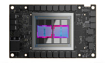
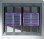
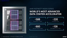
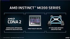
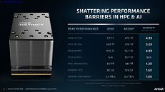
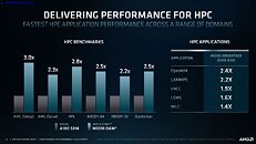
AMD's MI250X accelerator features two compute dies with 58 Billion transistors built out of TSMC's 6 nm process. Each of these chips features a total of 110 Compute Units (CUs) for a total of 220 CUs on a single accelerator. The new CDNA2 architecture also incorporates new, improved Matrix Cores to the tune of 880 units (440 per chip). And as the MI250X is configured, that incredible amount of GPU power is paired with 128 GB of HBM2E memory, running at 3.2 TB/s. AMD's performance estimates against NVIDIA's current-gen A100 are blowouts. Compared to the A100, the MI250X is quoted as being: 4.9 times faster at FP64 vector compute; 2.5 times as fast in FP 32 Vector; 4.9 times faster in FP64 Matrix; a more meager 1.2 times faster performance on FP16 and BF16 Matrix operations; 1.6 times bigger memory capacity (128 GB on the MI 250X compared to the A100's 80 GB); and a 1.6 times faster memory bandwidth (though that's derived from the faster HBM2E memory).
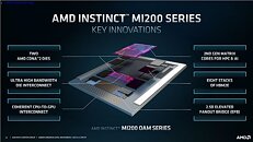
The two CDNA2 dies are linked together AMD's Infinity Fabric, which makes its debut on a graphics architecture. This link provides a series of 25 Gbps links offering up to 100 GB/s of bi-directional bandwidth between both GPUs. There are eight available links in the MI200's distribution module - built to the specifications of an OAM (OCP Accelerator Module, where OCP stands for "Open Compute Platform") configuration. In total 800 GB/s of bandwidth are available for on-the fly communication between the two chiplets. AMD already announced that a PCIe version of the MI200 is launching in the future, catering to those who just want drop-in replacements or upgrades.
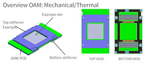
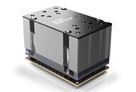
AMD's usage of TSMC's N6 fabrication technology can certainly account for part of the performance and die size improvement. As any manufacturer will do, AMD is employing yield optimizing efforts. This becomes clear when we look at the other product AMD is introducing alongside the MI250X: the MI250 accelerator. The MI250 takes a hit on computational resources by dropping from the MI250X's 110 CUs to 104 CUs per chiplet. That's actually the only change; it should be around 5% slower than the fully-enabled MI250X.
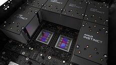
All in all, the MI200 series is a marked improvement for AMD performance-wise. And yet, NVIDIA is sure to announce their own next-generation compute solution soon. How will the updated, CDNA2-powered MI200 series stand?
View at TechPowerUp Main Site


AMD's MI250X accelerator features two compute dies with 58 Billion transistors built out of TSMC's 6 nm process. Each of these chips features a total of 110 Compute Units (CUs) for a total of 220 CUs on a single accelerator. The new CDNA2 architecture also incorporates new, improved Matrix Cores to the tune of 880 units (440 per chip). And as the MI250X is configured, that incredible amount of GPU power is paired with 128 GB of HBM2E memory, running at 3.2 TB/s. AMD's performance estimates against NVIDIA's current-gen A100 are blowouts. Compared to the A100, the MI250X is quoted as being: 4.9 times faster at FP64 vector compute; 2.5 times as fast in FP 32 Vector; 4.9 times faster in FP64 Matrix; a more meager 1.2 times faster performance on FP16 and BF16 Matrix operations; 1.6 times bigger memory capacity (128 GB on the MI 250X compared to the A100's 80 GB); and a 1.6 times faster memory bandwidth (though that's derived from the faster HBM2E memory).


The two CDNA2 dies are linked together AMD's Infinity Fabric, which makes its debut on a graphics architecture. This link provides a series of 25 Gbps links offering up to 100 GB/s of bi-directional bandwidth between both GPUs. There are eight available links in the MI200's distribution module - built to the specifications of an OAM (OCP Accelerator Module, where OCP stands for "Open Compute Platform") configuration. In total 800 GB/s of bandwidth are available for on-the fly communication between the two chiplets. AMD already announced that a PCIe version of the MI200 is launching in the future, catering to those who just want drop-in replacements or upgrades.


AMD's usage of TSMC's N6 fabrication technology can certainly account for part of the performance and die size improvement. As any manufacturer will do, AMD is employing yield optimizing efforts. This becomes clear when we look at the other product AMD is introducing alongside the MI250X: the MI250 accelerator. The MI250 takes a hit on computational resources by dropping from the MI250X's 110 CUs to 104 CUs per chiplet. That's actually the only change; it should be around 5% slower than the fully-enabled MI250X.

All in all, the MI200 series is a marked improvement for AMD performance-wise. And yet, NVIDIA is sure to announce their own next-generation compute solution soon. How will the updated, CDNA2-powered MI200 series stand?
View at TechPowerUp Main Site


 .
. 


 Acts of charity and all that, lol.