Raevenlord
News Editor
- Joined
- Aug 12, 2016
- Messages
- 3,755 (1.20/day)
- Location
- Portugal
| System Name | The Ryzening |
|---|---|
| Processor | AMD Ryzen 9 5900X |
| Motherboard | MSI X570 MAG TOMAHAWK |
| Cooling | Lian Li Galahad 360mm AIO |
| Memory | 32 GB G.Skill Trident Z F4-3733 (4x 8 GB) |
| Video Card(s) | Gigabyte RTX 3070 Ti |
| Storage | Boot: Transcend MTE220S 2TB, Kintson A2000 1TB, Seagate Firewolf Pro 14 TB |
| Display(s) | Acer Nitro VG270UP (1440p 144 Hz IPS) |
| Case | Lian Li O11DX Dynamic White |
| Audio Device(s) | iFi Audio Zen DAC |
| Power Supply | Seasonic Focus+ 750 W |
| Mouse | Cooler Master Masterkeys Lite L |
| Keyboard | Cooler Master Masterkeys Lite L |
| Software | Windows 10 x64 |
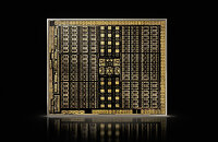
Renowned hardware leaker kopike7kimi on Twitter revealed some purported details on NVIDIA's next-generation architecture for HPC (High Performance Computing), Hopper. According to the leaker, Hopper is still sporting a classic monolithic die design despite previous rumors, and it appears that NVIDIA's performance targets have led to the creation of a monstrous, ~1000 mm² die package for the GH100 chip, which usually maxes out the complexity and performance that can be achieved on a particular manufacturing process. This is despite the fact that Hopper is also rumored to be manufactured under TSMC's 5 nm technology, thus achieving higher transistor density and power efficiency compared to the 8 nm Samsung process that NVIDIA is currently contracting. At the very least, it means that the final die will be bigger than the already enormous 826 mm² of NVIDIA's GA100.
If this is indeed the case and NVIDIA isn't deploying a MCM (Multi-Chip Module) design on Hopper, which is designed for a market with increased profit margins, it likely means that less profitable consumer-oriented products from NVIDIA won't be featuring the technology either. MCM designs also make more sense in NVIDIA's HPC products, as they would enable higher theoretical performance when scaling - exactly what that market demands. Of course, NVIDIA could be looking to develop an MCM version of the GH100 still; but if that were to happen, the company could be looking to pair two of these chips together as another HPC product (rumored GH-102). ~2,000 mm² in a single GPU package, paired with increased density and architectural improvements might actually be what NVIDIA requires to achieve the 3x performance jump from the Ampere-based A100 the company is reportedly targeting.

View at TechPowerUp Main Site
If this is indeed the case and NVIDIA isn't deploying a MCM (Multi-Chip Module) design on Hopper, which is designed for a market with increased profit margins, it likely means that less profitable consumer-oriented products from NVIDIA won't be featuring the technology either. MCM designs also make more sense in NVIDIA's HPC products, as they would enable higher theoretical performance when scaling - exactly what that market demands. Of course, NVIDIA could be looking to develop an MCM version of the GH100 still; but if that were to happen, the company could be looking to pair two of these chips together as another HPC product (rumored GH-102). ~2,000 mm² in a single GPU package, paired with increased density and architectural improvements might actually be what NVIDIA requires to achieve the 3x performance jump from the Ampere-based A100 the company is reportedly targeting.

View at TechPowerUp Main Site


