- Joined
- Aug 19, 2017
- Messages
- 2,929 (1.05/day)
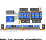
During the International Solid-State Circuits Conference (ISSCC) 2022, Intel gave us a more significant look at its upcoming Ponte Vecchio HPC accelerator and how it operates. So far, Intel convinced us that the company created Ponte Vecchio out of 47 tiles glued together in one package. However, the ISSCC presentation shows that the accelerator is structured rather interestingly. There are 63 tiles in total, where 16 are reserved for compute, eight are used for RAMBO cache, two are Foveros base tiles, two represent Xe-Link tiles, eight are HBM2E tiles, and EMIB connection takes up 11 tiles. This totals for about 47 tiles. However, an additional 16 thermal tiles used in Ponte Vecchio regulate the massive TDP output of this accelerator.
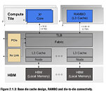
What is interesting is that Intel gave away details of the RAMBO cache. This novel SRAM technology uses four banks of 3.75 MB groups total of 15 MB per tile. They are connected to the fabric at 1.3 TB/s connection per chip. In contrast, compute tiles are connected at 2.6 TB/s speeds to the chip fabric. With eight RAMBO cache tiles, we get an additional 120 MB SRAM present. The base tile is a 646 mm² die manufactured in Intel 7 semiconductor process and contains 17 layers. It includes a memory controller, the Fully Integrated Voltage Regulators (FIVR), power management, 16-lane PCIe 5.0 connection, and CXL interface. The entire area of Ponte Vecchio is rather impressive, as 47 active tiles take up 2,330 mm², whereas when we include thermal dies, the total area jumps to 3,100 mm². And, of course, the entire package is much larger at 4,844 mm², connected to the system with 4,468 pins.

Intel chose TSMC's N5 node for compute tiles, while the Xe-Link tiles use the TSMC N7 node. For RAMBO cache and Foveros base tiles, Intel 7 process is used. The entire chip is designed for maximum efficiency and performance and has a TDP of 450 Watts for air cooling, while the water cooling enables it to boost TDP to 600 Watts. Ponte Vecchio is designed for 63-81°C operation—a standard requirement for this type of product used in HPC sector.
View at TechPowerUp Main Site | Source
What is interesting is that Intel gave away details of the RAMBO cache. This novel SRAM technology uses four banks of 3.75 MB groups total of 15 MB per tile. They are connected to the fabric at 1.3 TB/s connection per chip. In contrast, compute tiles are connected at 2.6 TB/s speeds to the chip fabric. With eight RAMBO cache tiles, we get an additional 120 MB SRAM present. The base tile is a 646 mm² die manufactured in Intel 7 semiconductor process and contains 17 layers. It includes a memory controller, the Fully Integrated Voltage Regulators (FIVR), power management, 16-lane PCIe 5.0 connection, and CXL interface. The entire area of Ponte Vecchio is rather impressive, as 47 active tiles take up 2,330 mm², whereas when we include thermal dies, the total area jumps to 3,100 mm². And, of course, the entire package is much larger at 4,844 mm², connected to the system with 4,468 pins.


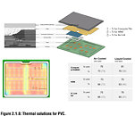
Intel chose TSMC's N5 node for compute tiles, while the Xe-Link tiles use the TSMC N7 node. For RAMBO cache and Foveros base tiles, Intel 7 process is used. The entire chip is designed for maximum efficiency and performance and has a TDP of 450 Watts for air cooling, while the water cooling enables it to boost TDP to 600 Watts. Ponte Vecchio is designed for 63-81°C operation—a standard requirement for this type of product used in HPC sector.

View at TechPowerUp Main Site | Source


 Just to catch up on cross-die latency.
