- Joined
- Oct 9, 2007
- Messages
- 47,582 (7.46/day)
- Location
- Dublin, Ireland
| System Name | RBMK-1000 |
|---|---|
| Processor | AMD Ryzen 7 5700G |
| Motherboard | ASUS ROG Strix B450-E Gaming |
| Cooling | DeepCool Gammax L240 V2 |
| Memory | 2x 8GB G.Skill Sniper X |
| Video Card(s) | Palit GeForce RTX 2080 SUPER GameRock |
| Storage | Western Digital Black NVMe 512GB |
| Display(s) | BenQ 1440p 60 Hz 27-inch |
| Case | Corsair Carbide 100R |
| Audio Device(s) | ASUS SupremeFX S1220A |
| Power Supply | Cooler Master MWE Gold 650W |
| Mouse | ASUS ROG Strix Impact |
| Keyboard | Gamdias Hermes E2 |
| Software | Windows 11 Pro |
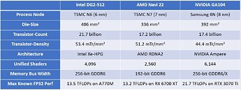
Some interesting technical specifications of the elusive two GPUs behind the Intel Arc "Alchemist" series surfaced. The larger DG2-512 silicon in particular, which forms the base for the Arc 5 and Arc 7 series, is interesting, in that it is larger in every way than the performance-segment ASICs from both NVIDIA and AMD. The table below compares the physical specs of the DG2-512, with the NVIDIA GA104, and the AMD Navi 22. This segment of GPUs has fairly powerful use-cases, including native 1440p gameplay, or playing at 4K with a performance enhancement—something Intel has, in the form of the XeSS.
The DG2-512 is built on the 6 nm TSMC N6 foundry node, the most advanced node among the three GPUs in this class. It has the highest transistor density of 53.4 mTr/mm², and the largest die-area of 406 mm², and the highest transistor-count of 21.7 billion. The Xe-HPG graphics architecture is designed for full DirectX 12 Ultimate feature support, and the DG2-512 dedicated hardware for ray tracing, as well as AI acceleration. The Arc A770M is the fastest product based on this silicon, however, it is a mobile GPU with aggressive power-management characteristic to the form-factor it serves. Here, the DG2-512 has an FP32 throughput of 13.5 TFLOPs, compared to 13.2 TFLOPs of the Navi 22 on the Radeon RX 6700 XT desktop graphics card, and the 21.7 TFLOPs of the GA104 that's maxed out on the GeForce RTX 3070 Ti desktop graphics card.

View at TechPowerUp Main Site | Source
The DG2-512 is built on the 6 nm TSMC N6 foundry node, the most advanced node among the three GPUs in this class. It has the highest transistor density of 53.4 mTr/mm², and the largest die-area of 406 mm², and the highest transistor-count of 21.7 billion. The Xe-HPG graphics architecture is designed for full DirectX 12 Ultimate feature support, and the DG2-512 dedicated hardware for ray tracing, as well as AI acceleration. The Arc A770M is the fastest product based on this silicon, however, it is a mobile GPU with aggressive power-management characteristic to the form-factor it serves. Here, the DG2-512 has an FP32 throughput of 13.5 TFLOPs, compared to 13.2 TFLOPs of the Navi 22 on the Radeon RX 6700 XT desktop graphics card, and the 21.7 TFLOPs of the GA104 that's maxed out on the GeForce RTX 3070 Ti desktop graphics card.

View at TechPowerUp Main Site | Source


