- Joined
- Aug 19, 2017
- Messages
- 2,897 (1.04/day)
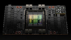
During the GTC 2022 keynote, NVIDIA announced its newest addition to the accelerator cards family. Called NVIDIA H100 accelerator, it is the company's most powerful creation ever. Utilizing 80 billion of TSMC's 4N 4 nm transistors, H100 can output some insane performance, according to NVIDIA. Featuring a new fourth-generation Tensor Core design, it can deliver a six-fold performance increase compared to A100 Tensor Cores and a two-fold MMA (Matrix Multiply Accumulate) improvement. Additionally, new DPX instructions accelerate Dynamic Programming algorithms up to seven times over the previous A100 accelerator. Thanks to the new Hopper architecture, the Streaming Module structure has been optimized for better transfer of large data blocks.
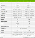
The full GH100 chip implementation features 144 SMs, and 128 FP32 CUDA cores per SM, resulting in 18,432 CUDA cores at maximum configuration. The NVIDIA H100 GPU with SXM5 board form-factor features 132 SMs, totaling 16,896 CUDA cores, while the PCIe 5.0 add-in card has 114 SMs, totaling 14,592 CUDA cores. As much as 80 GB of HBM3 memory surrounds the GPU at 3 TB/s bandwidth. Interestingly, the SXM5 variant features a very large TDP of 700 Watts, while the PCIe card is limited to 350 Watts. This is the result of better cooling solutions offered for the SXM form-factor. As far as performance figures are concerned, the SXM and PCIe versions provide two distinctive figures for each implementation. You can check out the performance estimates in various precision modes below. You can read more about the Hopper architecture and what makes it special in this whitepaper published by NVIDIA.


View at TechPowerUp Main Site
The full GH100 chip implementation features 144 SMs, and 128 FP32 CUDA cores per SM, resulting in 18,432 CUDA cores at maximum configuration. The NVIDIA H100 GPU with SXM5 board form-factor features 132 SMs, totaling 16,896 CUDA cores, while the PCIe 5.0 add-in card has 114 SMs, totaling 14,592 CUDA cores. As much as 80 GB of HBM3 memory surrounds the GPU at 3 TB/s bandwidth. Interestingly, the SXM5 variant features a very large TDP of 700 Watts, while the PCIe card is limited to 350 Watts. This is the result of better cooling solutions offered for the SXM form-factor. As far as performance figures are concerned, the SXM and PCIe versions provide two distinctive figures for each implementation. You can check out the performance estimates in various precision modes below. You can read more about the Hopper architecture and what makes it special in this whitepaper published by NVIDIA.


View at TechPowerUp Main Site


