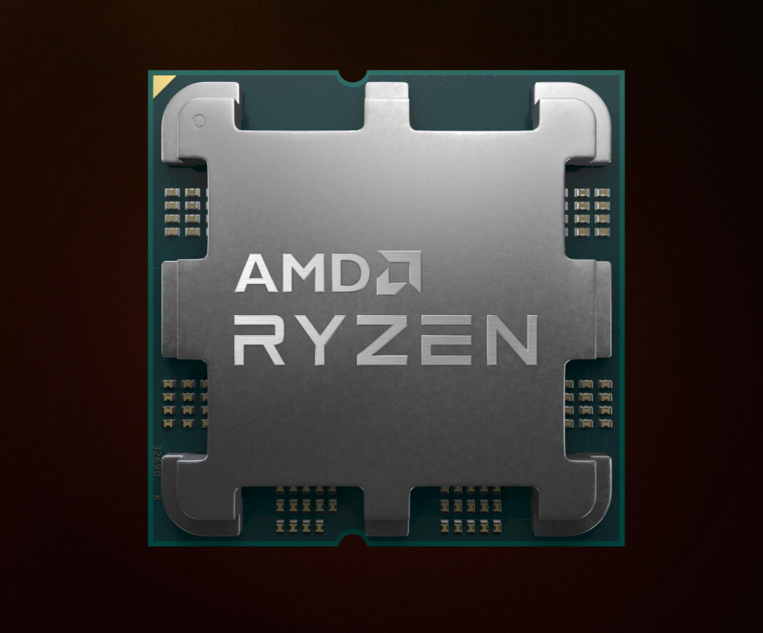
It's definitely have that shape to avoid getting bent.
My guess is that the cutouts are an efficient way to get more area from the package available for components,
where the contact area against the package in
yellow is probably thinner and not glued.
Red = glued areas.
Blue = space available for chips.
View attachment 243720
Compare with AM4, where the glued part takes up more space.
View attachment 243721
The AM5 design basically have more area available which is equal to all the cutouts together, more or less.
The goal was to minimize the glued area, which is unusable for both SMD's and chips.


")