- Joined
- Oct 9, 2007
- Messages
- 47,598 (7.45/day)
- Location
- Dublin, Ireland
| System Name | RBMK-1000 |
|---|---|
| Processor | AMD Ryzen 7 5700G |
| Motherboard | Gigabyte B550 AORUS Elite V2 |
| Cooling | DeepCool Gammax L240 V2 |
| Memory | 2x 16GB DDR4-3200 |
| Video Card(s) | Galax RTX 4070 Ti EX |
| Storage | Samsung 990 1TB |
| Display(s) | BenQ 1440p 60 Hz 27-inch |
| Case | Corsair Carbide 100R |
| Audio Device(s) | ASUS SupremeFX S1220A |
| Power Supply | Cooler Master MWE Gold 650W |
| Mouse | ASUS ROG Strix Impact |
| Keyboard | Gamdias Hermes E2 |
| Software | Windows 11 Pro |
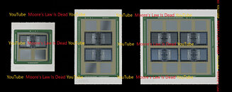
AMD's next-generation MI300 compute accelerator is expected to significantly scale up the logic density, according to a rumor by Moore's Law is Dead. Based on the CDNA3 compute architecture, the MI300 will be a monstrous large multi-chip module with as many as 8 logic dies (compute dies), each with its dedicated HBM3 stack. The compute dies (logic dies), will be 3D-stacked on top of I/O dies that pack the memory controllers, and the interconnect that performs the inter-die, and inter-package communication.
The report even goes on to mention that the compute die at the top level of the stack will be built on TSMC N5 (5 nm) silicon fabrication process, while the I/O die below will be TSMC N6 (6 nm). At this point it's not known if AMD will use the package to wire the logic stacks to the memory stacks, or whether it will take the pricier route of using a silicon interposer, but the report supports the interposer theory—that an all-encompassing interposer seats all eight compute dies, all four I/O dies (each with two compute dies), and the eight HBM3 stacks. An interposer is a silicon die that facilitates high density microscopic wiring between two dies on a package, which are otherwise not possible through large package substrate wiring.


View at TechPowerUp Main Site | Source
The report even goes on to mention that the compute die at the top level of the stack will be built on TSMC N5 (5 nm) silicon fabrication process, while the I/O die below will be TSMC N6 (6 nm). At this point it's not known if AMD will use the package to wire the logic stacks to the memory stacks, or whether it will take the pricier route of using a silicon interposer, but the report supports the interposer theory—that an all-encompassing interposer seats all eight compute dies, all four I/O dies (each with two compute dies), and the eight HBM3 stacks. An interposer is a silicon die that facilitates high density microscopic wiring between two dies on a package, which are otherwise not possible through large package substrate wiring.


View at TechPowerUp Main Site | Source


