- Joined
- Oct 9, 2007
- Messages
- 47,293 (7.53/day)
- Location
- Hyderabad, India
| System Name | RBMK-1000 |
|---|---|
| Processor | AMD Ryzen 7 5700G |
| Motherboard | ASUS ROG Strix B450-E Gaming |
| Cooling | DeepCool Gammax L240 V2 |
| Memory | 2x 8GB G.Skill Sniper X |
| Video Card(s) | Palit GeForce RTX 2080 SUPER GameRock |
| Storage | Western Digital Black NVMe 512GB |
| Display(s) | BenQ 1440p 60 Hz 27-inch |
| Case | Corsair Carbide 100R |
| Audio Device(s) | ASUS SupremeFX S1220A |
| Power Supply | Cooler Master MWE Gold 650W |
| Mouse | ASUS ROG Strix Impact |
| Keyboard | Gamdias Hermes E2 |
| Software | Windows 11 Pro |
NVIDIA designed the Grace CPU, a processor in the classical sense, to replace the Intel Xeon or AMD EPYC processors it was having to cram into its pre-built HPC compute servers for serial-processing roles, and mainly because those half-a-dozen GPU HPC processors need to be interconnected by a CPU. The company studied the CPU-level limitations and bottlenecks not just with I/O, but also the machine-architecture, and realized its compute servers need a CPU purpose-built for the role, with an architecture that's heavily optimized for NVIDIA's APIs. This, the NVIDIA Grace CPU was born.
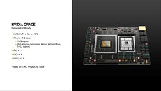
This is NVIDIA's first outing with a CPU with a processing footprint rivaling server processors from Intel and AMD. Built on the TSMC N4 (4 nm EUV) silicon fabrication process, it is a monolithic chip that's deployed standalone with an H100 HPC processor on a single board that NVIDIA calls a "Superchip." A board with a Grace and an H100, makes up a "Grace Hopper" Superchip. A board with two Grace CPUs makes a Grace CPU Superchip. Each Grace CPU contains a 900 GB/s switching fabric, a coherent interface, which has seven times the bandwidth of PCI-Express 5.0 x16. This is key to connecting the companion H100 processor, or neighboring Superchips on the node, with coherent memory access.

Serial processing muscle on the NVIDIA Grace CPU is care of a 72-core Arm v9 64-bit CPU. A Superchip would contain 144 cores. The main memory interface is LPDDR5x, with each "socket" having a maximum memory bandwidth of 1 TB/s (or rivaling that of over 24 channels of DDR5). This includes ECC. A key serial-IO interface is PCI-Express Gen 5, with 68 lanes on offer. These are mainly to wire out NVMe storage devices. The chip has a TDP rating of 500 W peak.
The Grace CPU demonstrates the engineering muscle of NVIDIA at designing large multi-core processors for enterprise and HPC applications. With Arm achieving near-parity with x86-64 in performance, efficiency, and IPC, we're beginning to understand why NVIDIA couldn't become an x86 licensee. It would have achieved a winning enterprise processor rivaling Intel's much before. Future generations of NVIDIA's DGX compute nodes, as well as pre-built workstations and servers, spanning a multitude of applications, could see NVIDIA wean away from x86-based CPUs, replacing them with Grace and its successors.
View at TechPowerUp Main Site | Source
This is NVIDIA's first outing with a CPU with a processing footprint rivaling server processors from Intel and AMD. Built on the TSMC N4 (4 nm EUV) silicon fabrication process, it is a monolithic chip that's deployed standalone with an H100 HPC processor on a single board that NVIDIA calls a "Superchip." A board with a Grace and an H100, makes up a "Grace Hopper" Superchip. A board with two Grace CPUs makes a Grace CPU Superchip. Each Grace CPU contains a 900 GB/s switching fabric, a coherent interface, which has seven times the bandwidth of PCI-Express 5.0 x16. This is key to connecting the companion H100 processor, or neighboring Superchips on the node, with coherent memory access.

Serial processing muscle on the NVIDIA Grace CPU is care of a 72-core Arm v9 64-bit CPU. A Superchip would contain 144 cores. The main memory interface is LPDDR5x, with each "socket" having a maximum memory bandwidth of 1 TB/s (or rivaling that of over 24 channels of DDR5). This includes ECC. A key serial-IO interface is PCI-Express Gen 5, with 68 lanes on offer. These are mainly to wire out NVMe storage devices. The chip has a TDP rating of 500 W peak.
The Grace CPU demonstrates the engineering muscle of NVIDIA at designing large multi-core processors for enterprise and HPC applications. With Arm achieving near-parity with x86-64 in performance, efficiency, and IPC, we're beginning to understand why NVIDIA couldn't become an x86 licensee. It would have achieved a winning enterprise processor rivaling Intel's much before. Future generations of NVIDIA's DGX compute nodes, as well as pre-built workstations and servers, spanning a multitude of applications, could see NVIDIA wean away from x86-based CPUs, replacing them with Grace and its successors.
View at TechPowerUp Main Site | Source


