• Welcome to TechPowerUp Forums, Guest! Please check out our forum guidelines for info related to our community.
  • The forums have been upgraded with support for dark mode. By default it will follow the setting on your system/browser. You may override it by scrolling to the end of the page and clicking the gears icon.

Intel "Raptor Lake" 8P+16E Wafer Pictured

btarunr

Editor & Senior Moderator
Staff member
Joined
Oct 9, 2007
Messages
47,852 (7.39/day)
Location
Dublin, Ireland
System Name RBMK-1000
Processor AMD Ryzen 7 5700G
Motherboard Gigabyte B550 AORUS Elite V2
Cooling DeepCool Gammax L240 V2
Memory 2x 16GB DDR4-3200
Video Card(s) Galax RTX 4070 Ti EX
Storage Samsung 990 1TB
Display(s) BenQ 1440p 60 Hz 27-inch
Case Corsair Carbide 100R
Audio Device(s) ASUS SupremeFX S1220A
Power Supply Cooler Master MWE Gold 650W
Mouse ASUS ROG Strix Impact
Keyboard Gamdias Hermes E2
Software Windows 11 Pro
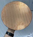
Andreas Schilling with Hardwareluxx.de, as part of the Intel Tech Tour Israel, got to hold a 12-inch wafer full of "Raptor Lake-S" dies. These are dies in their full 8P+16E configuration. The die is estimated to measure 257 mm² in area. We count 231 full dies on this wafer. Intel is building "Raptor Lake" on the same 10 nm Enhanced SuperFin (aka Intel 7) node as "Alder Lake." The die is about 23% larger than "Alder Lake" on account of two additional E-core clusters, possibly larger P-cores, and larger L2 caches for both the P-core and E-core clusters. "Raptor Lake" gains significance as it will be the last client processor from Intel to be built on a monolithic die of a uniform silicon fabrication node. Future generations are expected to take the chiplets route, realizing the company's IDM 2.0 product development strategy.


View at TechPowerUp Main Site | Source
 
big chip for a CPU.
 
Can someone explain to me what's the point of making chips on the edge of the wafer? Even making a mask for exposing those parts seems to make no sense to me.
Edge of a waffel is always more tasty.
 
This was also leaked:


Summary:
1-3% IPC increase from ADL to RPL
2-4% IPC advantage RPL over Zen4
Not much change going from DDR5 4800 to DDR5 6000 for both companies
Gracemont sucks at floating point instructions
 
Can someone explain to me what's the point of making chips on the edge of the wafer? Even making a mask for exposing those parts seems to make no sense to me.
No idea why they do it. I would have thought they could print other (smaller) chips which would mean free chips and less wafer wasted. Also, the grid is suboptimal. By staggering the chips, ie not on a square grid, but on a staggered grid, they could have a lot less waste. Example. Look down the middle row. Two “80%” cpus are wasted. By staggering/offset, you could have one extra CPU and two 30% cpus wasted. Better patent that idea quick.
 
Can someone explain to me what's the point of making chips on the edge of the wafer? Even making a mask for exposing those parts seems to make no sense to me.
Even if they're only partial chips, they give the wafer uniformity in thickness and tension so stress cracks are much less likely to develop during dicing.
 
No idea why they do it. I would have thought they could print other (smaller) chips which would mean free chips and less wafer wasted. Also, the grid is suboptimal. By staggering the chips, ie not on a square grid, but on a staggered grid, they could have a lot less waste. Example. Look down the middle row. Two “80%” cpus are wasted. By staggering/offset, you could have one extra CPU and two 30% cpus wasted. Better patent that idea quick.
No expert, but clearly the production method requires cutting a circular shape of silicon into chips. It's not a question about "making" the ones at the end or not - they just are there once the wafer has been processed anyway. At this point in time it is safe to assume that waste courtesy of the production process as such has been minimized. If square wafers were an option they would have been implemented a long time ago.
 
What are those areas on the wafer that look like stains? Are those bad dies?
 
Even if they're only partial chips, they give the wafer uniformity in thickness and tension so stress cracks are much less likely to develop during dicing.
Wafers with unprocessed partial chips were a common sight years ago. It's hard to find a photo of one from the last decade (where age can be confirmed). However, I found a wafer of Meteor Lake test chips from 2021 here, and is not processed to the edge.
Is there more than one dicing method used in the industry?

Can someone explain to me what's the point of making chips on the edge of the wafer? Even making a mask for exposing those parts seems to make no sense to me.
With some luck, that's how you get those processors with F suffix, haha.
 
I'll take a slice of that pizza, extra Wattage & cheese please
 
Forgive my ignorance, but what happens to the unusable chips along the edges of the wafer?

Is that silicon able to be recycled/reused on future wafers, or are they just thrown away as part of the cost of business?
 
Can someone explain to me what's the point of making chips on the edge of the wafer? Even making a mask for exposing those parts seems to make no sense to me.
I've always wondered that too! Why make the system waste it's time on those areas of the wafer?

Forgive my ignorance, but what happens to the unusable chips along the edges of the wafer?
Garbage.
 
Can someone explain to me what's the point of making chips on the edge of the wafer? Even making a mask for exposing those parts seems to make no sense to me.
Because the clarity of focus decreases at the edges. So if they focus to only printing at the center of the wafer then the clarity around the edge of the print will still be fuzzier than in the very center, and they'll lose those dies to distortions/imperfections in the print. So what they do instead is have the entire wafer in focus and allow the outer edge where the focus is the worst to be sacrificial, while keeping the more complete dies on the inner portion of the wafer more in focus.

While EUV solves some of this portion by allowing the masks to block light with more clarity, the biggest problem with edge roughness comes from the photomasks involved. Very slight changes in light deflection during the process due to the exposure angle leads to one or multiple layered features on the less focused edge losing their integrity and being basically junk. While from a macro level these chips look the same, at the micro level they could have entire structures printed wrong, missing critical connections between oxide layers, or have many small wire defects where the connecting wires were not printed to the proper size or fused with their neighbors.

Also not every mask set includes the edge of the wafer. In prior generation lithography techniques there's sometimes less desire to print to the edges for lead-time (time to manufacture and ship) reasons if yields are of little concern. Smaller ICs like those for networking, DACs, media encoder ASICs, or hobbyist FPGAs made on older nodes don't need to be as worried about detail preservation. In part due to those lithography machines being exceptionally well tuned by now, and also due to many of those types of ICs being relatively simple in design with many fewer masks per print with less chance of egregious errors in the process.
 
Last edited:
Because the clarity of focus decreases at the edges. So if they focus to only printing at the center of the wafer then the clarity around the edge of the print will still be fuzzier than in the very center, and they'll lose those dies to distortions/imperfections in the print. So what they do instead is have the entire wafer in focus and allow the outer edge where the focus is the worst to be sacrificial, while keeping the more complete dies on the inner portion of the wafer more in focus.

While EUV solves some of this portion by allowing the masks to block light with more clarity, the biggest problem with edge roughness comes from the photomasks involved. Very slight changes in light deflection during the process due to the exposure angle leads to one or multiple layered features on the less focused edge losing their integrity and being basically junk. While from a macro level these chips look the same, at the micro level they could have entire structures printed wrong, missing critical connections between oxide layers, or have many small wire defects where the connecting wires were not printed to the proper size or fused with their neighbors.

Also not every mask set includes the edge of the wafer. In prior generation lithography techniques there's sometimes less desire to print to the edges for lead-time (time to manufacture and ship) reasons if yields are of little concern. Smaller ICs like those for networking, DACs, media encoder ASICs, or hobbyist FPGAs made on older nodes don't need to be as worried about detail preservation. In part due to those lithography machines being exceptionally well tuned by now, and also due to many of those types of ICs being relatively simple in design with many fewer masks per print with less chance of egregious errors in the process.
You're describing the exposure as if it were a one-step process but that's not how it goes.

A small portion at a time is exposed to UV light. It can be one die if it's very large, or several smaller dies, with a total size no larger than 26 x 33 mm (the reticle size). The wafer moves between the exposures - it's mounted on a trolley with linear motors that move it across a flat surface. The optical system is stationary. One exposure takes a couple tenths of a second, and the movement (with nanometer precision!) takes about as much time too. Partial chips at the edge take as much time as whole chips and it would be better to skip them - but there are good reasons to not skip them, already explained in this thread.

So all exposures across the wafer are equally sharp. However, exposure is far from being the only critical step in manufacturing. There's deposition, baking, polishing, cleaning and so on. Blank wafer manufacturing too, of course. Some of these steps may not be perfectly uniform across the wafer. Best quality dies are usually near the center if I remember correctly.

Forgive my ignorance, but what happens to the unusable chips along the edges of the wafer?

Is that silicon able to be recycled/reused on future wafers, or are they just thrown away as part of the cost of business?
There's a guy called Ian Cutress, he's the right guy to answer this question, and breakfast time is the best time to ask him.

What are those areas on the wafer that look like stains? Are those bad dies?
Yes. On a wafer held in bare hands like this, all dies are bad dies. Even those without obvious fingerprints.
 
Can someone explain to me what's the point of making chips on the edge of the wafer? Even making a mask for exposing those parts seems to make no sense to me.

2 core, 4 core, 8 core chips say hello.
 
2 core, 4 core, 8 core chips say hello.
Like majority of those chips have their entire IO die cut off or half of it. Pretty sure that's not how those cpu's happen.
 
2 core, 4 core, 8 core chips say hello.
You forgot 3.14159 core chips.

Well, maybe those partial chips are useful for destructive testing. Measurement and checking is done many times during the ~3 months of wafer manufacturing, and if some testing method requires the chip to be destroyed (for example, by grinding or etching layers away), it's cheaper to do it on a chip that will never work anyway. In addition, these chips can be exposed with less or more UV radiation, and then analysed to see if the dose needs to be adjusted for the rest of the batch of wafers.
 
Back
Top