• Welcome to TechPowerUp Forums, Guest! Please check out our forum guidelines for info related to our community.

AMD Radeon RX 7900 XTX RDNA3 Prototype Leaked, Confirms Reference Cooler Design

If the 7900XTX is only taking up 2.5, maybe we'll see the 7900XT in 2 slot. The 7800XT should definitely be. I'm really impressed with the size considering.
I hope so, I just need a dual slot card for my setup and don’t want to lose my pci e x1 card!
 
Yes, but this is the 7900XTX. Would be a bit surprising if the XTX has the same TBP as the XT. Although there is historical precedent for it going back to the R9 290 and 290X ;)
We don't know if this is the XTX or XT. The source of this leak said nothing to confirm which specific card this is, and to my knowledge we don't have any other information to go on. The article headline is making an assumption and presenting it as fact, which is unfortunately common with this particular author.

The XTX may have three 8-pins or at least two 8-pins and a 6-pin.
 
A traditional color for prototypes. Nothing new about this, the electronics industry has been doing this for decades.
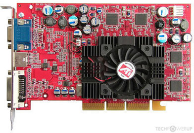
ATi's PCBs use to be red.

 
I have this card. No reason to go and kill it(sell it) for 15 euros. Unfortunately the previous owner had already removed the sticker from the cooler. On the other hand it's not bad looking considering it's transparent.

Fun part about the previous owner and an example of average consumer.
15+ years ago he wanted a system to use his PCI satellite card. So I had build him a system with good enough CPU and RAM and chose a simple HD 2400 Pro for the graphics card, thinking he isn't playing games. Huge mistake, it wasn't capable of 1080p satelite channel playback. So, I tell him to go and ask the shop to replace that card with an HD 2600, thinking that card will be enough. He instead gone and bought the strongest AMD there was. The HD 3870 just to playback video streams from the satellite card. Maybe one of the few HD 3870's that didn't run a 3D game for at least a decade.
 
There were some very VERY specific reasons for that (AMD got what was wrong with the process and took that into account when designing). It is unreasonable to expect that sort of advantage this time.
That ignores the history of AMD's evergreen. AMD's HD 2000, 3000, and 4000 series were all focus on small, efficient dies that were performance competitive with nvidia. The AMD HD 4870 traded blows with the GTX 280, the 280 was a 576mm2 die, the 4870 was 256mm2. It's not unreasonable at all to think that AMD has used some of their newfound profits and increased R+D to heavily optimize rDNA3.

I don't trust these numbers.
NV went 10752 => 16384 so, plus 52%.
AMD going 5120 => 12288 would be plus 140%

Most likely AMD simply got into NV marketing "business" of claiming twice the number of shaders they really have (since they could do fp+fp is the formal reason for this lie).

So in real numbers, AMD is going from 5120 to 6140 real cores, an increase of 20%.
Hmmm......Do you think that AMD is dumb enough to put 24GB of RAM on a warmed over 6900xt? Would they use a chiplet design but hold themselves back to dies the size of a 6700xt? I doubt it.
 
Thats 20mm to long for Meshify C setup - damn

View attachment 267967

Btw @Wizzard could you include in your upcomming test if thermalpads on the back plate is needed like on the reference 6900/6950XT and how thick it need to bee.
Can`t you mount the radiator on top as exhaust and add 2 fans in front instead as intake?
My bad, after a closer inspection I have seen the size of that rad.
 
Can`t you mount the radiator on top as exhaust and add 2 fans in front instead as intake?
My bad, after a closer inspection I have seen the size of that rad.
That's no rad, that's a car radiator!
 
That's no rad, that's a car radiator!
Back to our roots!

Wonder how long until a case maker thinks to integrate a radiator into a case design...
 
Back to our roots!

Wonder how long until a case maker thinks to integrate a radiator into a case design...
Already done! I also bet there is more! https://www.tomshardware.com/news/regner-1700-euro-water-cooling-case
1667309624438.png
 
  • Haha
Reactions: ARF
It's really shit. To the point where they stopped selling them. der8auer has many videos on it.
Yeah thats a little pricy. A good radiator is only $200 for a big one, I was thinking more along the lines of a HAF case or similar with a 240/280mm rad built in.
 
Hmmm......Do you think that AMD is dumb enough to put 24GB of RAM on a warmed over 6900xt? Would they use a chiplet design but hold themselves back to dies the size of a 6700xt? I doubt it.

They were on par last gen.
10752 is marketing BS, real number is 5376 (yes, they can do fp+fp, that doesn't double their number) vs 5120 by AMD.

Especially with die size in mind, AMD going with +20% shaders is 10+ times more probable, than AMD going with magical +140%.

The latter is simply technically impossible, how the heck do you cram that into that chip?

+20% shaders also aligns well with only 2 8 pin connectors (so 375W max).
So nvidia going from 5376 cores to 8192 cores (a 2816 core, or over 50%) increase while also pulling less power according to sites like TPU and techspot is perfectly fine, but AMD is only going to go up by 20% total? Wat?

That's some pretty narrow tunnel vision there.
 
So nvidia going from 5376 cores to 8192 cores (a 2816 core, or over 50%) increase while also pulling less power according to sites like TPU and techspot is perfectly fine, but AMD is only going to go up by 20% total? Wat?

That's some pretty narrow tunnel vision there.

It's also blatantly wrong because Nvidia does actually have 16384 shaders on the 4090 and 10496 on the 3090ti.
 
So nvidia going from 5376 cores to 8192 cores (a 2816 core, or over 50%) increase while also pulling less power according to sites like TPU and techspot is perfectly fine, but AMD is only going to go up by 20% total?
Did you just compare apples to oranges? Core increase to power increase? What the heck?
("pulling less power" per TPU just shows how lacking TPUs "power pulling" testing is, but that's beside the point)

NV went from 5376 cores to 8192 cores, a 50% increase, and created new bazinga connector to feed the beast.

AMD rolling out only two 8-pin connectors perfectly aligns with 20% increase in shaders over 6950XT.

5700XT was 2560 cores. A card that was merely high range. 6950XT is only 2 times that.

140% (2.4 times) increase gen over gen, while sitting on two 8-pins is not even remotely imaginable.

Nvidia does actually have 16384
No, it doesn't. Starting with 3000 series, Huang decided to claim twice the number of shaders the card had.
Not that Huang's claims needed anything of substance to support it (e.g. 4000 are "2-4 times faster"), but formal reason was that new shaders could do fp+fp, so they "should be counted as 2". It is still one shader (a dumb mini CPU)
 
Ugh give me a real dual slot card PLEASE
Reference 6800 and i hope 7800 also the same,
FE 2080 Ti, 3080s, 4080 (anything below xx90) and 3090 Turbo (asus/gigabyte) xD
 
No, it doesn't. Starting with 3000 series, Huang decided to claim twice the number of shaders the card had.
Not that Huang's claims needed anything of substance to support it (e.g. 4000 are "2-4 times faster"), but formal reason was that new shaders could do fp+fp, so they "should be counted as 2". It is still one shader (a dumb mini CPU)

No, they are 2 separate units entirely. In fact, they are groups of units.
cmFtLmpwZw

Where, on this, is a shader? Those listed cores don't have any scheduling logic like a CPU has, that's up in the warp scheduler. No instruction or data cache, that's in the register file and instruction buffer(and L1, obviously).

From a CPU perspective, nvidia has 4 cores per SM on maxwell, pascal(bar GP100), Turing, Ampere, and Lovelace.

So, ok, we've established that shaders are not similar to CPU cores, on maxwell here a shader is a unit that can do FP32 math, it's an FPU. How do we know that it's just FP32 math? Well the load/store units there would be akin to an AGU, they request and store data, which does do math but not the same type of math. And the Special Function Units handle more complex math like Sine transforms, which use things other than standard FP32.

So nvidia uses FP32 units for its shader counts, great. Now lets address your claim that Ampere uses 2 paired FPUs to reach the 128 shaders per SM number(note that such is the same number Maxwell and gaming Pascal reach).

LnBuZw

As you can see, the general structure remains the same, though there are changes carried over from Turing(fewer SFUs, LD/ST units closer to the cache, cache moved locations along with the SFUs, etc).

As you can also see, there are 2 datapaths in each SM subsection, 8 in total. One of these datapaths only does FP32 math while the other can do both, but it does both by having INT32 and FP32 units(ALUs and FPUs) on the same scheduling system, pairing them together but keeping the actual hardware units separate(likely for ease of design or for lower power draw, possibly to ease the next issue I'll talk about). Previous to Turing, all shaders were set up like this which caused some issues with context switching, that being the SM would take a few cycles(upwards of 10) to swap to an integer instruction and then take another few cycles to swap back to FP instructions.

With Ampere they decided to keep the split structures from Turing but added in more FP only units, as only around 30% of instructions are integer it makes sense to have only 1/3 of the SM be ALUs rather than the 1/2 Turing has. Ideally what they'd do is split INT off into its own datapath again, but it's possible that the extra die size incurred from such a move makes the economics infeasible or those INT units are primarily for doing tasks that the FPUs stall on and so it wouldn't gain much performance.

AMD, meanwhile, defines them similarly:
dC5qcGc

This is a Vega 20 compute unit, or CU, as found in the Mi50 and Mi60 datacenter cards.

They specifically call out Vector ALUs, or groups of FPUs and ALUs all paired together on the same datapath. Vega splits them up into subunits 4 units of 16 each and 2 major units of 32 each. This was changed in RDNA in that they merged 2 of the 16 wide units into one, getting a single 32 wide one and then pairing those into groups of 4(the WGPs).

But, still, the definitions are the same. 1 Shader=1 32bit FPU.

also: All shaders can do 2 floating point operations per clock cycle. All of them. That's why the formula to calculate tflops is Shaders*2*Clockspeed
 
No, they are 2 separate units entirely.

It's just semantic games about "CUs".

2080Ti, 4352 CUs
3080, 8704 "CUs" <= faux ones, apparently

So, 3080 had:
  1. "twice as many" CUs, that also "have higher IPC"
  2. was clocked higher
  3. had faster memory
But GPU performance of 3080 vs 2080Ti went ahead by just 25/30%

What does this performance gain align well with? Oh yeah, the same number of CUs with a small IPC bump (nowhere 1.4 times claimed by NV though) and higher clock.
 
It's just semantic games about "CUs".

The fuck is a "CU"? That's an AMD term, boy.

2080Ti, 4352 CUs
3080, 8704 "CUs" <= faux ones, apparently

Wut? They're real shaders. Each one does 2 FP32 ops per clock.

So, 3080 had:
  1. "twice as many" CUs, that also "have higher IPC"
  2. was clocked higher
  3. had faster memory
But GPU performance of 3080 vs 2080Ti went ahead by just 25/30%
What does this performance gain align well with? Oh yeah, the same number of CUs with a small IPC bump (nowhere 1.4 times claimed by NV though) and higher clock.

Nvidia never claimed higher performance per core for Ampere. That was maxwell, which you'd know if you bothered to fucking read the slide. It was literally right at the top, you can't miss it.

The performance per shader went down with Ampere, which is an entirely normal and expected behavior and one that Nvidia has had before with Kepler. They even tell you what a shader core is in kepler within its white paper:
SMX Processing Core Architecture Each of the Kepler GK110/210 SMX units feature 192 single-precision CUDA cores, and each core has fully pipelined floating-point and integer arithmetic logic units. Kepler retains the full IEEE 754-2008 compliant single- and double-precision arithmetic introduced in Fermi, including the fused multiply-add (FMA) operation.

If you look at the specs, a GTX 580 should be a lot slower than the GTX 760... but it isn't, it's only 6% slower according to TPU. Even looking at the tflops it should be slower than that, 1.58 vs 2.378

Going down in per shader performance almost always correlates with adding more shaders, because nothing scales perfectly. I'd expect a 30-40% gain in performance from a naive doubling of shaders, more if you double a lot of supporting structures with it.

If you do it perfectly, you'd scale up to what your front end allows, but this isn't always possible because you'd need to sacrifice a lot of area for routing logic, so you'd not be able to double shaders overall making scaling gains moot.
 
i dont think that amd's reference model cant beat rtx 4090,not even close,but AIB models,top of them,with tdp 450W ,can come close,but not RT performance.

i wonder,if amd launch rdna3 gpus today,do we see also review of them?

i hope...but if so,example Techpowerup know alot now,all of it.

they have both cards at least few days now, and reviews are done.
 
Back
Top