- Joined
- Oct 9, 2007
- Messages
- 47,611 (7.45/day)
- Location
- Dublin, Ireland
| System Name | RBMK-1000 |
|---|---|
| Processor | AMD Ryzen 7 5700G |
| Motherboard | Gigabyte B550 AORUS Elite V2 |
| Cooling | DeepCool Gammax L240 V2 |
| Memory | 2x 16GB DDR4-3200 |
| Video Card(s) | Galax RTX 4070 Ti EX |
| Storage | Samsung 990 1TB |
| Display(s) | BenQ 1440p 60 Hz 27-inch |
| Case | Corsair Carbide 100R |
| Audio Device(s) | ASUS SupremeFX S1220A |
| Power Supply | Cooler Master MWE Gold 650W |
| Mouse | ASUS ROG Strix Impact |
| Keyboard | Gamdias Hermes E2 |
| Software | Windows 11 Pro |
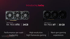
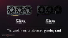
AMD today announced the Radeon RX 7900 XTX and Radeon RX 7900 XT gaming graphics cards debuting its next-generation RDNA3 graphics architecture. The two new cards come at $999 and $899—basically targeting the $1000 high-end premium price point.
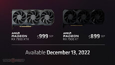
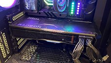
Both cards will be available on December 13th, not only the AMD reference design, which is sold through AMD.com, but also custom-design variants from the many board partners on the same day. AIBs are expected to announce their products in the coming weeks.
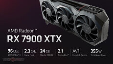
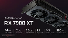
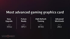
The RX 7900 XTX is priced at USD $999, and the RX 7900 XT is $899, which is a surprisingly small difference of only $100, for a performance difference that will certainly be larger, probably in the 20% range. Both Radeon RX 7900 XTX and RX 7900 XT are using the PCI-Express 4.0 interface, Gen 5 is not supported with this generation. The RX 7900 XTX has a typical board power of 355 W, or about 95 W less than that of the GeForce RTX 4090. The reference-design RX 7900 XTX uses conventional 8-pin PCIe power connectors, as would custom-design cards, when they come out. AMD's board partners will create units with three 8-pin power connectors, for higher out of the box performance and better OC potential. The decision to not use the 16-pin power connector that NVIDIA uses was made "well over a year ago", mostly because of cost, complexity and the fact that these Radeons don't require that much power anyway.
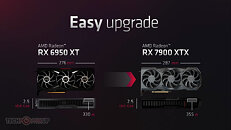
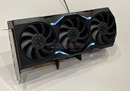
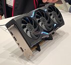
The reference RX 7900-series board design has the same card height as the RX 6950 XT, but is just 1 cm longer, at 28.7 cm. It is also strictly 2.5 slots thick. There's some white illuminated elements, which are controllable, using the same software as on the Radeon RX 6000 Series. Both cards feature two DisplayPort 2.1 outputs, one HDMI 2.1a and one USB-C.
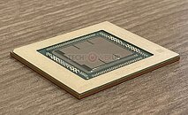
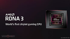
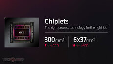
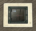
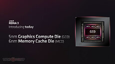
This is AMD's first attempt at a gaming GPU made of chiplets (multiple logic dies on a multi-chip module). The company has built MCM GPUs in the past, but those have essentially been the GPU die surrounded by HBM stacks. The new "Navi 31" GPU at the heart of the RX 7900 XTX and RX 7900 XT features seven chiplets—a central large graphics compute die (GCD), surrounded by six memory control-cache dies (MCDs). The GCD is built on the TSMC 5 nm EUV silicon fabrication process—the same one on which AMD builds its "Zen 4" CCDs—while the MCDs are each fabricated on the TSMC 6 nm process.

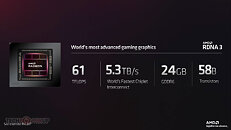
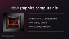
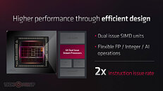
The GCD contains the GPU's main graphics rendering machinery, including the front-end, the RDNA3 compute units, the Ray Accelerators, the display controllers, the media engine and the render backends. The GCD physically features 96 RDNA3 Unified Compute Units (CUs), for 6,144 stream processors. All 96 of these are enabled on the RX 7900 XTX. The RX 7900 XT has 84 out of 96 unified compute units enabled, which works out to 5,376 stream processors. The new RDNA3 next-generation compute unit introduces dual-issue stream processors, which essentially double their throughput generation-over-generation. This is a VLIW approach, AMD does not double the rated shader count though, so it's 6144 for the full GPU (96 CU x 64 shaders per CU, not 128 shaders per CU).
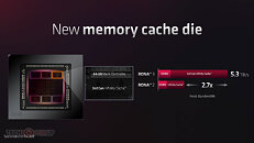
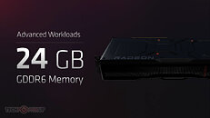
Each of the six MCDs contains a 64-bit wide GDDR6 memory interface, and 16 MB of Infinity Cache memory. Six of these MCDs add up to the GPU's 384-bit wide memory interface, and 96 MB of total Infinity Cache memory. The GCD addresses the 384-bit wide memory interface as a contiguous addressable block, and not 6x 64-bit. Most modern GPUs for the past decade have had multiple on-die memory controllers making up a larger memory interface, "Navi 31" moves these to separate chiplets. This approach reduces the size of the main GCD tile, which will help with yield rates. The Radeon RX 7900 XTX is configured with 24 GB of GDDR6 memory across the chip's entire 384-bit wide memory bus, while the RX 7900 XT gets 20 GB of GDDR6 memory across a 320-bit wide memory bus (one of the MCDs is disabled). The disabled MCD isn't not "missing", but there's some dummy silicon dies there to provide stability for the cooler mounting.

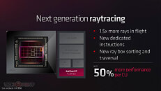
Each CU also features two AI acceleration components that provide a 2.7x uplift in AI inference performance over SIMD, and a second-generation RT accelerator that provides new dedicated instructions, and a 50% performance uplift in ray tracing performance. The AI cores are not exposed through software, software developers cannot use them directly (unlike NVIDIA's Tensor Cores), they are used exclusively by the GPU internal engines. Later today AMD will give us a more technical breakdown of the RDNA3 architecture.
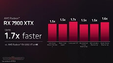
For the RX 7900 XTX, AMD is broadly claiming an up to 70% increase in traditional raster 3D graphics performance over the previous-generation flagship RX 6950 XT at 4K Ultra HD native resolution; and an up to 60% increase in ray tracing performance. These gains should be good to catch RTX 4080, but AMD was clear that they are not targeting RTX 4090 performance, which comes at a much higher price point, too.
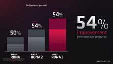
AMD is attributing its big 54% performance/Watt generational gains to a revolutionary asynchronous clock domain technology that runs the various components on the GCD at different frequencies, to minimize power draw. This seems similar in concept to the "shader clock" on some older NVIDIA architectures.
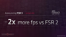
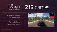
AMD also announced FSR 3.0, the latest generation of its performance enhancement, featuring Fluid Motion technology. This is functionally similar to DLSS 3 Frame Generation, promising a 100% uplift in performance at comparable quality—essentially because the GPU is generating every alternate frame without involving its graphics rendering pipeline.
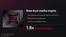
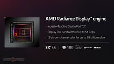
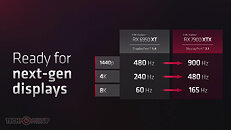
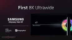
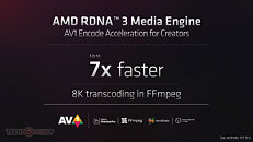
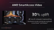
The new dual-independent media-acceleration engines enable simultaneous encode and decode for AVC and HEVC formats; hardware-accelerated encode and decode for AV1, and AI-accelerated enhancements. The new AMD Radiance Display Engine introduces native support for DisplayPort 2.1, with 54 Gbps display link bandwidth, and 12 bpc color. This enables resolutions of up to 8K @ 165 Hz with a single cable; or 4K @ 480 Hz with a single cable.
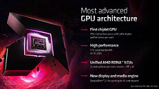
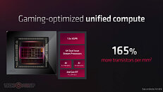
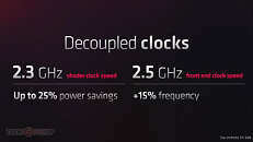
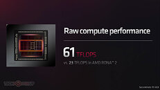
The "Navi 31" GPU in its full configuration has a raw compute throughput of 61 TFLOPs, compared to 23 TFLOPs of the RDNA2-based Navi 21 (a 165% increase). The shader and front-end of the GPU operate at different clock speeds, with the shaders running at up to 2.30 GHz, and the front-end at up to 2.50 GHz. This decoupling has a big impact on power-savings, with AMD claiming a 25% power-saving as opposed to running both domains at the same 2.50 GHz clock.
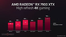
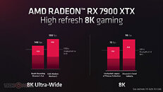
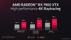
AMD claims the Radeon RX 7900 XTX to offer a 70% performance increase over the RX 6950 XT.
The complete slide-deck follows.


























View at TechPowerUp Main Site


Both cards will be available on December 13th, not only the AMD reference design, which is sold through AMD.com, but also custom-design variants from the many board partners on the same day. AIBs are expected to announce their products in the coming weeks.


The RX 7900 XTX is priced at USD $999, and the RX 7900 XT is $899, which is a surprisingly small difference of only $100, for a performance difference that will certainly be larger, probably in the 20% range. Both Radeon RX 7900 XTX and RX 7900 XT are using the PCI-Express 4.0 interface, Gen 5 is not supported with this generation. The RX 7900 XTX has a typical board power of 355 W, or about 95 W less than that of the GeForce RTX 4090. The reference-design RX 7900 XTX uses conventional 8-pin PCIe power connectors, as would custom-design cards, when they come out. AMD's board partners will create units with three 8-pin power connectors, for higher out of the box performance and better OC potential. The decision to not use the 16-pin power connector that NVIDIA uses was made "well over a year ago", mostly because of cost, complexity and the fact that these Radeons don't require that much power anyway.


The reference RX 7900-series board design has the same card height as the RX 6950 XT, but is just 1 cm longer, at 28.7 cm. It is also strictly 2.5 slots thick. There's some white illuminated elements, which are controllable, using the same software as on the Radeon RX 6000 Series. Both cards feature two DisplayPort 2.1 outputs, one HDMI 2.1a and one USB-C.


This is AMD's first attempt at a gaming GPU made of chiplets (multiple logic dies on a multi-chip module). The company has built MCM GPUs in the past, but those have essentially been the GPU die surrounded by HBM stacks. The new "Navi 31" GPU at the heart of the RX 7900 XTX and RX 7900 XT features seven chiplets—a central large graphics compute die (GCD), surrounded by six memory control-cache dies (MCDs). The GCD is built on the TSMC 5 nm EUV silicon fabrication process—the same one on which AMD builds its "Zen 4" CCDs—while the MCDs are each fabricated on the TSMC 6 nm process.


The GCD contains the GPU's main graphics rendering machinery, including the front-end, the RDNA3 compute units, the Ray Accelerators, the display controllers, the media engine and the render backends. The GCD physically features 96 RDNA3 Unified Compute Units (CUs), for 6,144 stream processors. All 96 of these are enabled on the RX 7900 XTX. The RX 7900 XT has 84 out of 96 unified compute units enabled, which works out to 5,376 stream processors. The new RDNA3 next-generation compute unit introduces dual-issue stream processors, which essentially double their throughput generation-over-generation. This is a VLIW approach, AMD does not double the rated shader count though, so it's 6144 for the full GPU (96 CU x 64 shaders per CU, not 128 shaders per CU).

Each of the six MCDs contains a 64-bit wide GDDR6 memory interface, and 16 MB of Infinity Cache memory. Six of these MCDs add up to the GPU's 384-bit wide memory interface, and 96 MB of total Infinity Cache memory. The GCD addresses the 384-bit wide memory interface as a contiguous addressable block, and not 6x 64-bit. Most modern GPUs for the past decade have had multiple on-die memory controllers making up a larger memory interface, "Navi 31" moves these to separate chiplets. This approach reduces the size of the main GCD tile, which will help with yield rates. The Radeon RX 7900 XTX is configured with 24 GB of GDDR6 memory across the chip's entire 384-bit wide memory bus, while the RX 7900 XT gets 20 GB of GDDR6 memory across a 320-bit wide memory bus (one of the MCDs is disabled). The disabled MCD isn't not "missing", but there's some dummy silicon dies there to provide stability for the cooler mounting.

Each CU also features two AI acceleration components that provide a 2.7x uplift in AI inference performance over SIMD, and a second-generation RT accelerator that provides new dedicated instructions, and a 50% performance uplift in ray tracing performance. The AI cores are not exposed through software, software developers cannot use them directly (unlike NVIDIA's Tensor Cores), they are used exclusively by the GPU internal engines. Later today AMD will give us a more technical breakdown of the RDNA3 architecture.


For the RX 7900 XTX, AMD is broadly claiming an up to 70% increase in traditional raster 3D graphics performance over the previous-generation flagship RX 6950 XT at 4K Ultra HD native resolution; and an up to 60% increase in ray tracing performance. These gains should be good to catch RTX 4080, but AMD was clear that they are not targeting RTX 4090 performance, which comes at a much higher price point, too.


AMD is attributing its big 54% performance/Watt generational gains to a revolutionary asynchronous clock domain technology that runs the various components on the GCD at different frequencies, to minimize power draw. This seems similar in concept to the "shader clock" on some older NVIDIA architectures.

AMD also announced FSR 3.0, the latest generation of its performance enhancement, featuring Fluid Motion technology. This is functionally similar to DLSS 3 Frame Generation, promising a 100% uplift in performance at comparable quality—essentially because the GPU is generating every alternate frame without involving its graphics rendering pipeline.


The new dual-independent media-acceleration engines enable simultaneous encode and decode for AVC and HEVC formats; hardware-accelerated encode and decode for AV1, and AI-accelerated enhancements. The new AMD Radiance Display Engine introduces native support for DisplayPort 2.1, with 54 Gbps display link bandwidth, and 12 bpc color. This enables resolutions of up to 8K @ 165 Hz with a single cable; or 4K @ 480 Hz with a single cable.

The "Navi 31" GPU in its full configuration has a raw compute throughput of 61 TFLOPs, compared to 23 TFLOPs of the RDNA2-based Navi 21 (a 165% increase). The shader and front-end of the GPU operate at different clock speeds, with the shaders running at up to 2.30 GHz, and the front-end at up to 2.50 GHz. This decoupling has a big impact on power-savings, with AMD claiming a 25% power-saving as opposed to running both domains at the same 2.50 GHz clock.


AMD claims the Radeon RX 7900 XTX to offer a 70% performance increase over the RX 6950 XT.
The complete slide-deck follows.


View at TechPowerUp Main Site


