- Joined
- Oct 9, 2007
- Messages
- 47,636 (7.44/day)
- Location
- Dublin, Ireland
| System Name | RBMK-1000 |
|---|---|
| Processor | AMD Ryzen 7 5700G |
| Motherboard | Gigabyte B550 AORUS Elite V2 |
| Cooling | DeepCool Gammax L240 V2 |
| Memory | 2x 16GB DDR4-3200 |
| Video Card(s) | Galax RTX 4070 Ti EX |
| Storage | Samsung 990 1TB |
| Display(s) | BenQ 1440p 60 Hz 27-inch |
| Case | Corsair Carbide 100R |
| Audio Device(s) | ASUS SupremeFX S1220A |
| Power Supply | Cooler Master MWE Gold 650W |
| Mouse | ASUS ROG Strix Impact |
| Keyboard | Gamdias Hermes E2 |
| Software | Windows 11 Pro |
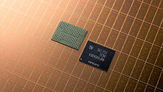
Samsung Electronics Co., Ltd., the world leader in advanced memory technology, as promised at Flash Memory Summit 2022 and Samsung Memory Tech Day 2022, announced today that it has begun mass producing a 1-terabit (Tb) triple-level cell (TLC) eighth-generation Vertical NAND (V-NAND) with the industry's highest bit density. At 1 Tb, the new V-NAND also features the highest storage capacity to date, enabling larger storage space in next-generation enterprise server systems worldwide.
"As market demand for denser, greater-capacity storage pushes for higher V-NAND layer counts, Samsung has adopted its advanced 3D scaling technology to reduce surface area and height, while avoiding the cell-to-cell interference that normally occurs with scaling down," said SungHoi Hur, Executive Vice President of Flash Product & Technology at Samsung Electronics. "Our eighth-generation V-NAND will help meet rapidly growing market demand and better position us to deliver more differentiated products and solutions, which will be at the very foundation of future storage innovations."

Samsung was able to attain the industry's highest bit density by significantly enhancing the bit productivity per wafer. Based on the Toggle DDR 5.0 interface—the latest NAND flash standard—Samsung's eighth-generation V-NAND features an input and output (I/O) speed of up to 2.4 gigabits per second (Gbps), a 1.2X boost over the previous generation. This will enable the new V-NAND to accommodate the performance requirements of PCIe 4.0, and later, PCIe 5.0.
The eighth-generation V-NAND is expected to serve as the cornerstone for storage configurations that help expand the storage capacity in next-generation enterprise servers, while extending its use into the automotive market where reliability is especially critical.
View at TechPowerUp Main Site
"As market demand for denser, greater-capacity storage pushes for higher V-NAND layer counts, Samsung has adopted its advanced 3D scaling technology to reduce surface area and height, while avoiding the cell-to-cell interference that normally occurs with scaling down," said SungHoi Hur, Executive Vice President of Flash Product & Technology at Samsung Electronics. "Our eighth-generation V-NAND will help meet rapidly growing market demand and better position us to deliver more differentiated products and solutions, which will be at the very foundation of future storage innovations."

Samsung was able to attain the industry's highest bit density by significantly enhancing the bit productivity per wafer. Based on the Toggle DDR 5.0 interface—the latest NAND flash standard—Samsung's eighth-generation V-NAND features an input and output (I/O) speed of up to 2.4 gigabits per second (Gbps), a 1.2X boost over the previous generation. This will enable the new V-NAND to accommodate the performance requirements of PCIe 4.0, and later, PCIe 5.0.
The eighth-generation V-NAND is expected to serve as the cornerstone for storage configurations that help expand the storage capacity in next-generation enterprise servers, while extending its use into the automotive market where reliability is especially critical.
View at TechPowerUp Main Site


