T0@st
News Editor
- Joined
- Mar 7, 2023
- Messages
- 2,884 (3.77/day)
- Location
- South East, UK
| System Name | The TPU Typewriter |
|---|---|
| Processor | AMD Ryzen 5 5600 (non-X) |
| Motherboard | GIGABYTE B550M DS3H Micro ATX |
| Cooling | DeepCool AS500 |
| Memory | Kingston Fury Renegade RGB 32 GB (2 x 16 GB) DDR4-3600 CL16 |
| Video Card(s) | PowerColor Radeon RX 7800 XT 16 GB Hellhound OC |
| Storage | Samsung 980 Pro 1 TB M.2-2280 PCIe 4.0 X4 NVME SSD |
| Display(s) | Lenovo Legion Y27q-20 27" QHD IPS monitor |
| Case | GameMax Spark M-ATX (re-badged Jonsbo D30) |
| Audio Device(s) | FiiO K7 Desktop DAC/Amp + Philips Fidelio X3 headphones, or ARTTI T10 Planar IEMs |
| Power Supply | ADATA XPG CORE Reactor 650 W 80+ Gold ATX |
| Mouse | Roccat Kone Pro Air |
| Keyboard | Cooler Master MasterKeys Pro L |
| Software | Windows 10 64-bit Home Edition |
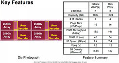
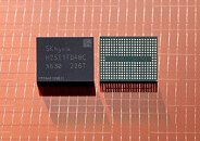
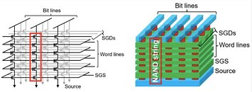
SK Hynix representatives unveiled the company's latest breakthrough in 3D NAND development at the ISSCC 2023 conference. Details of a new flash memory prototype featuring over 300 layers were revealed, and the company stated that a team of 35 engineers had contributed to the presentation material. In order to highlight the boost in performance offered by the prototype's improvements, it was compared to SK Hynix's previous record holding seventh-generation 238-layer 3D NAND. The new eighth-generation 3D NAND posted bandwidth figures with a maximum of 194 MB/s, which contrasts favorably with the older model's rate of 164 MB/s, representing an 18% increase in performance.
Recording density also benefits from the 300+ active layer design, with SK Hynix mentioning a 1 Tb (128 GB) capacity with triple level cells and a bit density of over 20 GB/mm^2. The chip features a 16 KB page size, four planes and a 2400 MT/s interface. The increase in density will result in a lower per-Tb cost during the manufacturing process. It is hoped that the end consumer will ultimately benefit from the boost in performance and capacity.
Five areas of technological implementations for the eighth-generation 3D NAND have been identified:
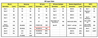
SK Hynix representatives did not provide any firm time frame for the production and eventual launch date of its cutting edge 3D NAND. Industry watchdogs have estimated that the memory boards will not reach shelves until very late 2024, or at some point in 2025. In the meantime, SK Hynix's seventh-generation 238-layer 3D NAND is expected to be integrated into the production cycle of new memory products due for release in 2023.


View at TechPowerUp Main Site | Source
Recording density also benefits from the 300+ active layer design, with SK Hynix mentioning a 1 Tb (128 GB) capacity with triple level cells and a bit density of over 20 GB/mm^2. The chip features a 16 KB page size, four planes and a 2400 MT/s interface. The increase in density will result in a lower per-Tb cost during the manufacturing process. It is hoped that the end consumer will ultimately benefit from the boost in performance and capacity.


Five areas of technological implementations for the eighth-generation 3D NAND have been identified:
- Triple-Verify Program (TPGM) feature that narrows cell threshold voltage distribution and reduces tPROG (program time) by 10%, which translates into higher performance
- Adaptive Unselected String Pre-Charge (AUSP) - another procedure to reduce tPROG by around 2%
- All-Pass Rising (APR) scheme that reduces tR (read time) by approximately 2% and cuts word line rising time
- Programmed Dummy String (PDS) technique that cuts world line settling time for tPROG and tR by reducing channel capacitance load
- Plane-Level Read Retry (PLRR) capability that allows to change read level of a plane without terminating others therefore issuing subsequent read commands immediately and improving quality of service (QoS) and therefore read performance

SK Hynix representatives did not provide any firm time frame for the production and eventual launch date of its cutting edge 3D NAND. Industry watchdogs have estimated that the memory boards will not reach shelves until very late 2024, or at some point in 2025. In the meantime, SK Hynix's seventh-generation 238-layer 3D NAND is expected to be integrated into the production cycle of new memory products due for release in 2023.


View at TechPowerUp Main Site | Source


