• Welcome to TechPowerUp Forums, Guest! Please check out our forum guidelines for info related to our community.

Intel "Emerald Rapids" Doubles Down on On-die Caches, Divests on Chiplets

btarunr

Editor & Senior Moderator
Staff member
Joined
Oct 9, 2007
Messages
46,891 (7.62/day)
Location
Hyderabad, India
System Name RBMK-1000
Processor AMD Ryzen 7 5700G
Motherboard ASUS ROG Strix B450-E Gaming
Cooling DeepCool Gammax L240 V2
Memory 2x 8GB G.Skill Sniper X
Video Card(s) Palit GeForce RTX 2080 SUPER GameRock
Storage Western Digital Black NVMe 512GB
Display(s) BenQ 1440p 60 Hz 27-inch
Case Corsair Carbide 100R
Audio Device(s) ASUS SupremeFX S1220A
Power Supply Cooler Master MWE Gold 650W
Mouse ASUS ROG Strix Impact
Keyboard Gamdias Hermes E2
Software Windows 11 Pro
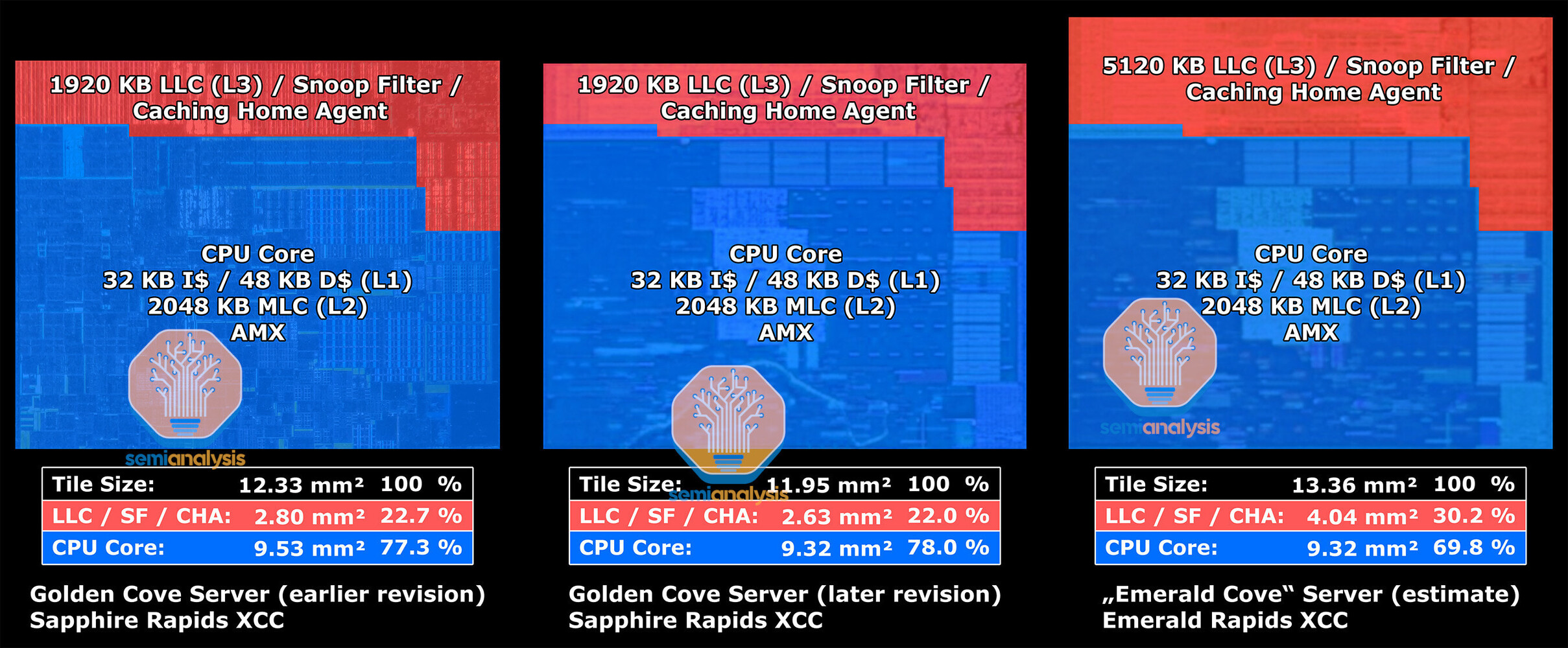
Finding itself embattled with AMD's EPYC "Genoa" processors, Intel is giving its 4th Gen Xeon Scalable "Sapphire Rapids" processor a rather quick succession in the form of the Xeon Scalable "Emerald Rapids," bound for Q4-2023 (about 8-10 months in). The new processor shares the same LGA4677 platform and infrastructure, and much of the same I/O, but brings about two key design changes that should help Intel shore up per-core performance, making it competitive to EPYC "Zen 4" processors with higher core-counts. SemiAnalysis compiled a nice overview of the changes, the two broadest points of it being—1. Intel is peddling back on the chiplet approach to high core-count CPUs, and 2., that it wants to give the memory sub-system and inter-core performance a massive performance boost using larger on-die caches.

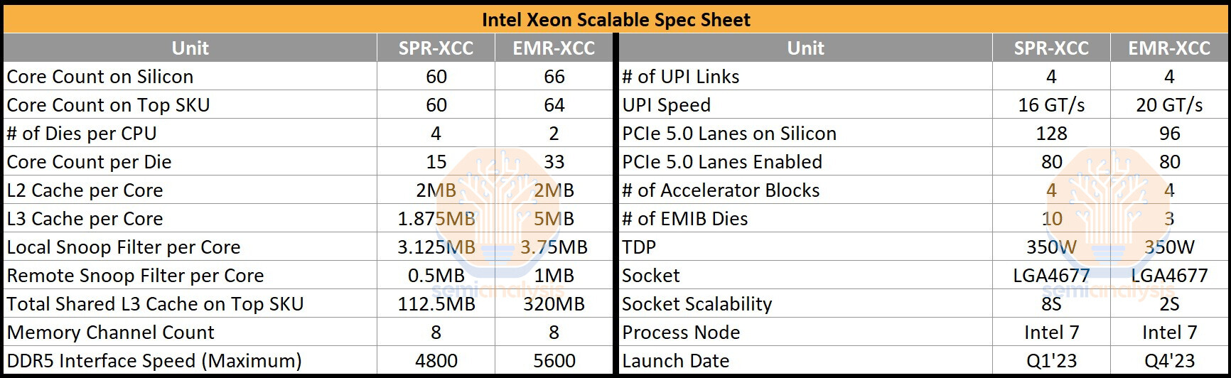
The "Emerald Rapids" processor has just two large dies in its extreme core-count (XCC) avatar, compared to "Sapphire Rapids," which can have up to four of these. There are just three EMIB dies interconnecting these two, compared to "Sapphire Rapids," which needs as many as 10 of these to ensure direct paths among the four dies. The CPU core count itself doesn't see a notable increase. Each of the two dies on "Emerald Rapids" physically features 33 CPU cores, so a total of 66 are physically present, although one core per die is left unused for harvesting, the SemiAnalysis article notes. So the maximum core-count possible commercially is 32 cores per die, or 64 cores per socket. "Emerald Rapids" continues to be based on the Intel 7 process (10 nm Enhanced SuperFin), probably with a few architectural improvements for higher clock-speeds.


As SemiAnalysis notes, the I/O is nearly identical between "Sapphire Rapids" and "Emerald Rapids." The processor puts out four 20 GT/s UPI links for inter-socket communication. Each of the two dies has a PCI-Express Gen 5 root-complex with 48 lanes, however only 40 of these are wired out. So the processor puts out a total of 80 PCIe Gen 5 lanes. This is an identical count to that of "Sapphire Rapids," which put out 32 lanes per chiplet, 128 in total, but only 20 lanes per die would be wired out. The memory interface is the same, with the processor featuring an 8-channel DDR5 interface, but the native memory speed sees an upgrade to DDR5-5600, up from the present DDR5-4800.

While "Sapphire Rapids" uses enterprise variants of the "Golden Cove" CPU cores that have 2 MB of dedicated L2 caches, "Emerald Rapids" use the more modern "Raptor Cove" cores that also power Intel's 13th Gen Core client processors. Each of the 66 cores has 2 MB of dedicated L2 cache. What's new, according to SemiAnalysis, is that each core has a large 5 MB segment of L3 cache, compared to "Golden Cove" enterprise, which only has a 1.875 MB segment, a massive 166% increase. The maximum amount of L3 cache possible on a 60-core "Sapphire Rapids" processor is 112.5 MB, whereas for the top 64-core "Emerald Rapids" SKU, this number is 320 MB, a 184% increase. Intel has also increased the cache snoop filter sizes per core.


SemiAnalysis also calculated that despite being based on the same Intel 7 process as "Sapphire Rapids," it would cost Intel less to make an "Emerald Rapids" processor with slightly higher core-count and much larger caches. Without scribe lines, the four dies making up "Sapphire Rapids" add up to 1,510 mm² of die-area, whereas the two dies making up "Emerald Rapids" only add up to 1,493 mm². Intel calculates that it can carve out all the relevant CPU core-count based SKUs by either giving the processor 1 or 2 dies, and doesn't need 4 of them for finer-grained SKU segmentation. AMD uses up to twelve 8-core "Zen 4" CCDs to achieve its 96-core count.

View at TechPowerUp Main Site | Source
 
Joined
Dec 12, 2016
Messages
1,530 (0.55/day)
This is quite a step back for Intel. There was a limited series Skylake Xeon some years back which included just two fused together 28 core dies. Emerald Rapids seems to be basically this concept again.

Also same die process, barely any increase in cores and only 2S doesn’t bode well so soon after Sapphire Rapids launch. Where is Aurora by the way?!?!
 
Joined
Sep 1, 2020
Messages
2,139 (1.48/day)
Location
Bulgaria
WoW! But what a fat cash cache! o_O
When in ordinary costumers segment?
 
Joined
Jan 3, 2021
Messages
3,081 (2.34/day)
Location
Slovenia
Processor i5-6600K
Motherboard Asus Z170A
Cooling some cheap Cooler Master Hyper 103 or similar
Memory 16GB DDR4-2400
Video Card(s) IGP
Storage Samsung 850 EVO 250GB
Display(s) 2x Oldell 24" 1920x1200
Case Bitfenix Nova white windowless non-mesh
Audio Device(s) E-mu 1212m PCI
Power Supply Seasonic G-360
Mouse Logitech Marble trackball, never had a mouse
Keyboard Key Tronic KT2000, no Win key because 1994
Software Oldwin
So Intel now thinks that mirrored dies were a bad idea.
 
Joined
Jun 1, 2021
Messages
247 (0.21/day)
Epyc-X will have 1,152 MB of L3 cache versus this 320 MB.
To be fair, memory access through CCDs are very slow, just as slow as going into main memory, so it's not like AMD has this huge block of 1152 MB of L3. In practice, it can really be a lot less.

Intel might have the same issues when going through one CPU die to another, but who knows.
 
Joined
Nov 4, 2005
Messages
11,867 (1.73/day)
System Name Compy 386
Processor 7800X3D
Motherboard Asus
Cooling Air for now.....
Memory 64 GB DDR5 6400Mhz
Video Card(s) 7900XTX 310 Merc
Storage Samsung 990 2TB, 2 SP 2TB SSDs, 24TB Enterprise drives
Display(s) 55" Samsung 4K HDR
Audio Device(s) ATI HDMI
Mouse Logitech MX518
Keyboard Razer
Software A lot.
Benchmark Scores Its fast. Enough.
Is Intel working on some magic they can’t figure out to get sub Nm soon or a different material that is preventing them from going beyond the 7super plus plus double good node?
 
Joined
May 25, 2014
Messages
275 (0.07/day)
any chance these will percolate down to the HEDT W790 platform, or just remain as non-W790 Xeons only
 
Last edited:

markhahn

New Member
Joined
May 3, 2023
Messages
2 (0.00/day)
Is Intel working on some magic they can’t figure out to get sub Nm soon or a different material that is preventing them from going beyond the 7super plus plus double good node?
The magic is called EUV.
 

markhahn

New Member
Joined
May 3, 2023
Messages
2 (0.00/day)
To be fair, memory access through CCDs are very slow, just as slow as going into main memory, so it's not like AMD has this huge block of 1152 MB of L3. In practice, it can really be a lot less.

Intel might have the same issues when going through one CPU die to another, but who knows.
Why do you think remote cache access is as slow as memory? A reference to measured latencies would be great...
 
Joined
Aug 12, 2022
Messages
231 (0.31/day)
Going from 4 core dies and 10 EMIB dies for Sapphire Rapids to 2 core dies and 3 EMIB dies for Emerald Rapids suggests a bottleneck somewhere in inter-die communication, a high cost for EMIB interconnects, or improving yields on the Intel 7 node.

I expect the extra cache and reduced number of dies will help in workloads that are highly threaded but also highly sensitive to core-to-core latency. That's an area I would expect Epyc to struggle with since Epyc has more core dies and nothing like EMIB for connecting them.
 
Joined
Aug 21, 2013
Messages
1,799 (0.45/day)
To be fair, memory access through CCDs are very slow, just as slow as going into main memory, so it's not like AMD has this huge block of 1152 MB of L3. In practice, it can really be a lot less.

Intel might have the same issues when going through one CPU die to another, but who knows.
This is much less of an issue in enterprise space as far as i understand. Most workloads are not latency sensitive like consumer workloads (gaming for example).
Besides i suspect for those workloads lower core count Epyc variants are better anyways due to less chiplets and higher clock speeds.
 
Joined
Dec 12, 2016
Messages
1,530 (0.55/day)
any chance these will percolate down to the HEDT W790 platform, or just remain as Xeons only
I would stay far away from Intel Xeons and HEDT for awhile. Something not right is going on with Intel’s enterprise products.
 
Joined
Jul 13, 2016
Messages
3,077 (1.04/day)
Processor Ryzen 7800X3D
Motherboard ASRock X670E Taichi
Cooling Noctua NH-D15 Chromax
Memory 32GB DDR5 6000 CL30
Video Card(s) MSI RTX 4090 Trio
Storage Too much
Display(s) Acer Predator XB3 27" 240 Hz
Case Thermaltake Core X9
Audio Device(s) Topping DX5, DCA Aeon II
Power Supply Seasonic Prime Titanium 850w
Mouse G305
Keyboard Wooting HE60
VR HMD Valve Index
Software Win 10
To be fair, memory access through CCDs are very slow, just as slow as going into main memory, so it's not like AMD has this huge block of 1152 MB of L3. In practice, it can really be a lot less.

Intel might have the same issues when going through one CPU die to another, but who knows.

A huge block of L3 cache would perform worse than the way way AMD has large amounts of cache localized to each CCD.

There are multiple problems with a single large cache, the first of which is that a single large cache is going to be much slower than a bunch of small caches (not that X3D cache is small, just in comparison to if you had added them together).

The 2nd bigger problem is that having a single large cache means that all the chips would have to fetch data from said cache. This is a problem design wise as not every chip is going to be equal distance from said cache and thus latencies increase the further away from the cache you get. You can see with RDNA2 and RDNA3 that AMD puts the L3 cache at both the top and bottom of the chip (whether that be on die or in the form of chiplets) in order to ensure a lower overall latency.

Having a 3D Cache chip on each CCD is vastly superior because it means that each CCD can localize all the data needed for work to be performed. The chiplet isn't wasting time and energy fetching data off die because it doesn't need to. We can see this from the energy efficiency of Zen 4 X3D chips and their performance in latency critical applications. In addition, due to how AMD stacks it's L3 on top you can put a ton of cache onto a chip while maintaining a lower latency that would otherwise be impossible if you tried to fit that cache onto a single chip. Now instead of a wire running halfway cross the chip on the X axis, you have a much smaller wire running on the Y axis.

So long as Intel isn't stacking it's cache AMD has an advantage in that regard.
 
Joined
Mar 18, 2023
Messages
749 (1.45/day)
System Name Never trust a socket with less than 2000 pins
any chance these will percolate down to the HEDT W790 platform, or just remain as Xeons only

The W690 CPUs are called Xeons, too. And they take registered RAM, so the only difference is the multi-processor configuration.
 
Joined
Jan 11, 2022
Messages
647 (0.68/day)
Are yields that good that they Can offer these big monolithic dies on intel 4?
 
Joined
Jun 1, 2021
Messages
247 (0.21/day)
This is much less of an issue in enterprise space as far as i understand. Most workloads are not latency sensitive like consumer workloads (gaming for example).
True, but was just commenting that the numbers might be way more than it actually is. Like how some archs use inclusive caches for their L3, which would that effective L3 is somewhat lower.
There are multiple problems with a single large cache, the first of which is that a single large cache is going to be much slower than a bunch of small caches (not that X3D cache is small, just in comparison to if you had added them together).
Those caches are generally implemented in slices, so no, you don't have a 'single large cache'. It's the reason why they put it at 5 MB/core as each L3 is a slice and a stop over the ringbus, which connects the cores to the rest of the system. And also, it's not simple to scale up with a lot of caches because of... coherence, which is one of the key point.
The 2nd bigger problem is that having a single large cache means that all the chips would have to fetch data from said cache.
This is even a bigger problem in AMD cache as said data can be off-chip which you have to access through the I/O die as there is no direct connection between the two chiplets.

I think you haven't thought of the coherence problem as say CORE#0 in Chiplet #0 has written something in Memory Address #XYZ, ofc, as per hierarchy it is first written to L1 and could eventually propagate in the hierarchy.

CORE#32 in Chiplet#5 wants to access the data in that same address. If L1/L2/L3(one of or more if inclusive) of CORE#0 still contains the data and hasn't written it to the main memory then that poses a problem as fetching it from the main memory would result in a wrong result. A simple solution would be to implement a write-through mechanism(i.e. you simply write to the memory whatever is written to the cache), but that could cause performance issue, though nothing that a lot of things do need to be written-through(e.g. peripherals that need to be updated now and not 'sometime in the future') so there are options to do it like caches flushes or mapping the same address twice, one passes through cache and other doesn't.

So the way that designers handle it is through bus snooping and/or directories. This shows how hard it is to implement chiplets as a mechanism to keep the coherence between the two or more really isn't going to be easy and should be the reason why CCD-to-CCD communication is very slow(it even shares the same 32B/cycle infinity fabric link that the CCD uses to communicate with the rest of the system, specially memory and really one of the big reasons why increasing IF clocks can improve perf in AMD processors).

That's not saying that Intel doesn't have a lot of challenges with L3 implementations and stuff. Alder Lake itself is known to reduce the ringbus clocks(same as L3 clocks) to the Gracemont cores when those are active, effectively slowing down the Goldmont cores L3 slices.

This is a problem design wise as not every chip is going to be equal distance from said cache and thus latencies increase the further away from the cache you get. You can see with RDNA2 and RDNA3 that AMD puts the L3 cache at both the top and bottom of the chip (whether that be on die or in the form of chiplets) in order to ensure a lower overall latency.

RDNA2/3 cache isn't the exact same. Specially for RDNA3 where they are together with the memory controller and so don't have a coherence problem, as it can only contain data specific to each memory controller. Probably one of the reasons why infinity cache is faster in RDNA3.
 
Joined
Jan 3, 2021
Messages
3,081 (2.34/day)
Location
Slovenia
Processor i5-6600K
Motherboard Asus Z170A
Cooling some cheap Cooler Master Hyper 103 or similar
Memory 16GB DDR4-2400
Video Card(s) IGP
Storage Samsung 850 EVO 250GB
Display(s) 2x Oldell 24" 1920x1200
Case Bitfenix Nova white windowless non-mesh
Audio Device(s) E-mu 1212m PCI
Power Supply Seasonic G-360
Mouse Logitech Marble trackball, never had a mouse
Keyboard Key Tronic KT2000, no Win key because 1994
Software Oldwin
Why do you think remote cache access is as slow as memory? A reference to measured latencies would be great...
Anandtech measured that in the Ryzen 9 7950X (and also 5950X for comparison):
They call it core-to-core latency but as far as I know, there is no method of directly sending signals or data from one core to another core. Rather, it's the latency when a core attempts to access data that is cached in a known location in the L3, in a slice of cache that belongs to another core. But that's alright, it's what matters here, and the latency across chiplets is ~77 ns.
 

hs4

Joined
Feb 15, 2022
Messages
106 (0.12/day)
Going from 4 core dies and 10 EMIB dies for Sapphire Rapids to 2 core dies and 3 EMIB dies for Emerald Rapids suggests a bottleneck somewhere in inter-die communication, a high cost for EMIB interconnects, or improving yields on the Intel 7 node.

I expect the extra cache and reduced number of dies will help in workloads that are highly threaded but also highly sensitive to core-to-core latency. That's an area I would expect Epyc to struggle with since Epyc has more core dies and nothing like EMIB for connecting them.
Basically, it is considered to be an improvement in yield. One post to AnandTech estimated that the yield at which an RPL B0 die could be used as a 13900K was about 90%, based on the ratio of F variants. Also, we rarely see i3-1215U and when it comes to Pentium 8505U we can hardly confirm its existence.

Applying these numbers, we can estimate that the yield at which all cores in the EMR can be activated is in the 60% range, and if we assume that one core is disabled, the yield is close to 90%.

The fact that Intel 10nm has significantly improved yield was commented on in the Q2 2021 financial report.
 
Joined
Jan 3, 2021
Messages
3,081 (2.34/day)
Location
Slovenia
Processor i5-6600K
Motherboard Asus Z170A
Cooling some cheap Cooler Master Hyper 103 or similar
Memory 16GB DDR4-2400
Video Card(s) IGP
Storage Samsung 850 EVO 250GB
Display(s) 2x Oldell 24" 1920x1200
Case Bitfenix Nova white windowless non-mesh
Audio Device(s) E-mu 1212m PCI
Power Supply Seasonic G-360
Mouse Logitech Marble trackball, never had a mouse
Keyboard Key Tronic KT2000, no Win key because 1994
Software Oldwin
Going from 4 core dies and 10 EMIB dies for Sapphire Rapids to 2 core dies and 3 EMIB dies for Emerald Rapids suggests a bottleneck somewhere in inter-die communication, a high cost for EMIB interconnects, or improving yields on the Intel 7 node.
Add packaging yields to the list. I'm just guessing here but the percentage of bad EMIBs in a large package might be considerable. How many Ponti Vecchi (Italian plural, hah) has Intel put together so far? Three of them?

Applying these numbers, we can estimate that the yield at which all cores in the EMR can be activated is in the 60% range, and if we assume that one core is disabled, the yield is close to 90%.
They don't even need those high yields. They have Xeons on sale with nearly any integer number of cores you can ask for, and probably there are enough HPC and server use cases which need the highest possible memory bandwidth and capacity, maybe PCIe lanes too, but not maximum processing power.
 
Joined
Dec 16, 2010
Messages
1,664 (0.33/day)
Location
State College, PA, US
System Name My Surround PC
Processor AMD Ryzen 9 7950X3D
Motherboard ASUS STRIX X670E-F
Cooling Swiftech MCP35X / EK Quantum CPU / Alphacool GPU / XSPC 480mm w/ Corsair Fans
Memory 96GB (2 x 48 GB) G.Skill DDR5-6000 CL30
Video Card(s) MSI NVIDIA GeForce RTX 4090 Suprim X 24GB
Storage WD SN850 2TB, 2 x 512GB Samsung PM981a, 4 x 4TB HGST NAS HDD for Windows Storage Spaces
Display(s) 2 x Viotek GFI27QXA 27" 4K 120Hz + LG UH850 4K 60Hz + HMD
Case NZXT Source 530
Audio Device(s) Sony MDR-7506 / Logitech Z-5500 5.1
Power Supply Corsair RM1000x 1 kW
Mouse Patriot Viper V560
Keyboard Corsair K100
VR HMD HP Reverb G2
Software Windows 11 Pro x64
Benchmark Scores Mellanox ConnectX-3 10 Gb/s Fiber Network Card
Going from 4 core dies and 10 EMIB dies for Sapphire Rapids to 2 core dies and 3 EMIB dies for Emerald Rapids suggests a bottleneck somewhere in inter-die communication, a high cost for EMIB interconnects, or improving yields on the Intel 7 node.

I expect the extra cache and reduced number of dies will help in workloads that are highly threaded but also highly sensitive to core-to-core latency. That's an area I would expect Epyc to struggle with since Epyc has more core dies and nothing like EMIB for connecting them.
Pretty sure that the major factor is the high cost/limited production of EMIB with a minor factor being improved yields on Intel 7. EMIB isn't a bottleneck in die-to-die communication; the move to fewer dies is simply to improve yield and production volume and to reduce costs.

Sapphire Rapids was Intel's first wide-release processor using EMIB (I'm not counting Ponte Vecchio because it sells orders of magnitude fewer CPUs than Xeons) and I suspect that they underestimated the cost of EMIB in wide deployment. Probably a combination of (relatively) low yields of chips using EMIB and production bottlenecks due to limited number of facilities that can assemble EMIB chips (compared to the number of 10nm fabs). Having fewer EMIB connections in chips means the existing EMIB facilities can assemble more chips. The tradeoff is a reduction of 10nm wafer yield (due to larger dies), but Intel is probably more equipped to handle the reduction in wafer yield because of the large number of facilities producing 10nm wafers.
 
Joined
Aug 12, 2022
Messages
231 (0.31/day)
Too bad it’s glued together :D
I believe Intel only made that claim about first-generation Epyc, which didn't perform well in unified memory uses. AMD implemented a better approach to unified memory with the second-generation Epyc. Moreover Intel's EMIB interconnects are a more performant form of interconnect (in theory) than what AMD uses today. I don't believe Intel ever described any of these newer architectures as "glued together".
Are yields that good that they Can offer these big monolithic dies on intel 4?
Emerald Rapids is going to be produced on the Intel 7 node.
 
Top