- Joined
- Aug 19, 2017
- Messages
- 3,242 (1.12/day)
The rumors of Nintendo's next-generation Switch handheld gaming console have been piling up ever since the competition in the handheld console market got more intense. Since the release of the original Switch, Valve has released Steam Deck, ASUS made ROG Ally, and others are also exploring the market. However, the next-generation Nintendo Switch 2 is closer and closer, as we have information about the chipset that will power this device. Thanks to Kepler_L2 on Twitter/X, we have the codenames of the upcoming processors. The first generation Switch came with NVIDIA's Tegra X1 SoC built on a 20 nm node. However, later on, NVIDIA supplied Nintendo with a Tegra X1+ SoC made on a 16 nm node. There were no performance increases recorded, just improved power efficiency. Both of them used four Cortex-A57 and four Cortex-A53 cores with GM20B Maxwell GPUs.
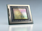
For the Nintendo Switch 2, NVIDIA is said to utilize a customized variant of NVIDIA Jetson Orin SoC for automotive applications. The reference Orin SoC carries a codename T234, while this alleged adaptation has a T239 codename; the version is most likely optimized for power efficiency. The reference Orin design is a considerable uplift compared to the Tegra X1, as it boasts 12 Cortex-A78AE cores and LPDDR5 memory, along with Ampere GPU microarchitecture. Built on Samsung's 8 nm node, the efficiency would likely yield better battery life and position the second-generation Switch well among the now extended handheld gaming console market. However, including Ampere architecture would also bring technologies like DLSS, which would benefit the low-power SoC.

View at TechPowerUp Main Site | Source
For the Nintendo Switch 2, NVIDIA is said to utilize a customized variant of NVIDIA Jetson Orin SoC for automotive applications. The reference Orin SoC carries a codename T234, while this alleged adaptation has a T239 codename; the version is most likely optimized for power efficiency. The reference Orin design is a considerable uplift compared to the Tegra X1, as it boasts 12 Cortex-A78AE cores and LPDDR5 memory, along with Ampere GPU microarchitecture. Built on Samsung's 8 nm node, the efficiency would likely yield better battery life and position the second-generation Switch well among the now extended handheld gaming console market. However, including Ampere architecture would also bring technologies like DLSS, which would benefit the low-power SoC.

View at TechPowerUp Main Site | Source


