- Joined
- Oct 9, 2007
- Messages
- 47,614 (7.45/day)
- Location
- Dublin, Ireland
| System Name | RBMK-1000 |
|---|---|
| Processor | AMD Ryzen 7 5700G |
| Motherboard | Gigabyte B550 AORUS Elite V2 |
| Cooling | DeepCool Gammax L240 V2 |
| Memory | 2x 16GB DDR4-3200 |
| Video Card(s) | Galax RTX 4070 Ti EX |
| Storage | Samsung 990 1TB |
| Display(s) | BenQ 1440p 60 Hz 27-inch |
| Case | Corsair Carbide 100R |
| Audio Device(s) | ASUS SupremeFX S1220A |
| Power Supply | Cooler Master MWE Gold 650W |
| Mouse | ASUS ROG Strix Impact |
| Keyboard | Gamdias Hermes E2 |
| Software | Windows 11 Pro |
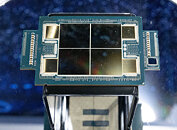
Intel CEO Pat Gelsinger, in the Q&A session of InnovatiON 2023 Day 1, confirmed that the company is developing 3D-stacked cache technology for its processors. The technology involves expanding the on-die last-level cache (L3 cache) of a processor with an additional SRAM die physically stacked on top, and bonded with the cache's high-bandwidth data fabric. The stacked cache operates at the same speed as the on-die cache, and so the combined cache size is visible to software as a single contiguous addressable block of cache memory.
AMD has used 3D-stacked cache to good effect on its processors. On client processors such as the Ryzen X3D series, the cache provides significant gaming performance uplifts as the larger L3 cache makes more of the game's rendering data immediately accessible to the CPU cores; while on server processors such as EPYC "Milan-X" and "Genoa-X," the added cache provides significant uplifts to memory intensive compute workloads. Intel's approach to 3D-stacked cache will be different at the hardware level compared to AMD's, Gelsinger stated in his response. AMD's tech has been collaboratively developed with TSMC, and hinges on a TSMC-made SoIC packaging tech that facilitates high-density die-to-die wiring between the CCD and cache chiplet. Intel uses its own fabs for processor dies, and will have to use its own IP.

"When you reference V-Cache, you're talking about a very specific technology that TSMC does with some of its customers as well. Obviously, we're doing that differently in our composition, right? And that particular type of technology isn't something that's part of Meteor Lake, but in our roadmap, you're seeing the idea of 3D silicon where we'll have cache on one die, and we'll have CPU compute on the stacked die on top of it, and obviously using EMIB that Foveros we'll be able to compose different capabilities," Gelsinger said.
"We feel very good that we have advanced capabilities for next-generation memory architectures, advantages for 3D stacking, for both little die, as well as for very big packages for AI and high-performance servers as well. So we have a full breadth of those technologies. We'll be using those for our products, as well as presenting it to the Foundry (IFS) customers as well," he added.
Intel recently provided an architecture deep-dive into its upcoming "Meteor Lake" client processor, in which its Foveros packaging tech and tile-to-tile interconnects allow the various tiles (chiplets) to work like a cohesive silicon. In particular, Intel appears to have solved the latency issues of having a the iGPU, CPU cores, and memory controllers on separate tiles.
View at TechPowerUp Main Site | Source
AMD has used 3D-stacked cache to good effect on its processors. On client processors such as the Ryzen X3D series, the cache provides significant gaming performance uplifts as the larger L3 cache makes more of the game's rendering data immediately accessible to the CPU cores; while on server processors such as EPYC "Milan-X" and "Genoa-X," the added cache provides significant uplifts to memory intensive compute workloads. Intel's approach to 3D-stacked cache will be different at the hardware level compared to AMD's, Gelsinger stated in his response. AMD's tech has been collaboratively developed with TSMC, and hinges on a TSMC-made SoIC packaging tech that facilitates high-density die-to-die wiring between the CCD and cache chiplet. Intel uses its own fabs for processor dies, and will have to use its own IP.

"When you reference V-Cache, you're talking about a very specific technology that TSMC does with some of its customers as well. Obviously, we're doing that differently in our composition, right? And that particular type of technology isn't something that's part of Meteor Lake, but in our roadmap, you're seeing the idea of 3D silicon where we'll have cache on one die, and we'll have CPU compute on the stacked die on top of it, and obviously using EMIB that Foveros we'll be able to compose different capabilities," Gelsinger said.
"We feel very good that we have advanced capabilities for next-generation memory architectures, advantages for 3D stacking, for both little die, as well as for very big packages for AI and high-performance servers as well. So we have a full breadth of those technologies. We'll be using those for our products, as well as presenting it to the Foundry (IFS) customers as well," he added.
Intel recently provided an architecture deep-dive into its upcoming "Meteor Lake" client processor, in which its Foveros packaging tech and tile-to-tile interconnects allow the various tiles (chiplets) to work like a cohesive silicon. In particular, Intel appears to have solved the latency issues of having a the iGPU, CPU cores, and memory controllers on separate tiles.
View at TechPowerUp Main Site | Source


 )
)


