- Joined
- Aug 19, 2017
- Messages
- 2,918 (1.05/day)
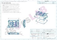
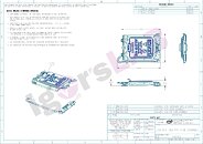
Thanks to the 3D renders and technical drawings obtained by Igor's Lab, we have insights into the structure of Intel's next-generation LGA-1851 socket for Arrow Lake processors. Scheduled to arrive in mid-2024, the LGA-1851 socket was originally intended for Meteor Lake-S desktop processors. However, the socket is now awaiting Arrow Lake since Meteor Lake is now a mobile-only processor generation. The first notable thing about LGA-1851 is that it will directly connect a dedicated PCIe 5.0 x4 interface to the CPU, besides the x16 lanes going to the GPU. This results in native support for high-speed PCIe 5.0 NVMe SSDs that can achieve speeds of over 12 GB/s in both read and write workloads.
Intel Arrow Lake-S will be available with eight P-cores and 16 E-cores in SKUs with different combinations of the two. The accompanying 800 series chipset includes Z890, B860, and H810 models, with an evident absence of H870 SKU. There will be W880 and Q870 workstation-grade chipsets as well. It is worth pointing out that Arrow Lake will enable DRAM capacities of up to 48 GB per DIMM at 6400 MT/s. We expect to hear more about Arrow Lake-S as we near the 2024 launch date and we get to see the Intel 20A node being used in client products. Below, you can see the technical drawings of the Independent Loading Mechanism (ILM) and chipset 3D models.

3D drawing of ILM and chipset.


Technical drawings of the LGA-1851 socket.


View at TechPowerUp Main Site | Source
Intel Arrow Lake-S will be available with eight P-cores and 16 E-cores in SKUs with different combinations of the two. The accompanying 800 series chipset includes Z890, B860, and H810 models, with an evident absence of H870 SKU. There will be W880 and Q870 workstation-grade chipsets as well. It is worth pointing out that Arrow Lake will enable DRAM capacities of up to 48 GB per DIMM at 6400 MT/s. We expect to hear more about Arrow Lake-S as we near the 2024 launch date and we get to see the Intel 20A node being used in client products. Below, you can see the technical drawings of the Independent Loading Mechanism (ILM) and chipset 3D models.

3D drawing of ILM and chipset.


Technical drawings of the LGA-1851 socket.


View at TechPowerUp Main Site | Source


