- Joined
- Aug 19, 2017
- Messages
- 2,929 (1.05/day)
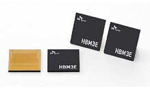
SK Hynix has unveiled ambitious High Bandwidth Memory (HBM) roadmaps at SEMICON Korea 2024. Vice President Kim Chun-hwan announced plans to mass produce the cutting-edge HBM3E within the first half of 2024, touting 8-layer stack samples already supplied to clients. This iteration makes major strides towards fulfilling surging data bandwidth demands, offering 1.2 TB/s per stack and 7.2 TB/s in a 6-stack configuration. VP Kim Chun-hwan cites the rapid emergence of generative AI, forecasted for 35% CAGR, as a key driver. He warns that "fierce survival competition" lies ahead across the semiconductor industry amidst rising customer expectations. With limits approaching on conventional process node shrinks, attention is shifting to next-generation memory architectures and materials to unleash performance.
SK Hynix has already initiated HBM4 development for sampling in 2025 and mass production the following year. According to Micron, HBM4 will leverage a wider 2048-bit interface compared to previous HBM generations to increase per-stack theoretical peak memory bandwidth to over 1.5 TB/s. To achieve these high bandwidths while maintaining reasonable power consumption, HBM4 is targeting a data transfer rate of around 6 GT/s. The wider interface and 6 GT/s speeds allow HBM4 to push bandwidth boundaries significantly compared to prior HBM versions, fueling the need for high-performance computing and AI workloads. But power efficiency is carefully balanced by avoiding impractically high transfer rates. Additionally, Samsung is aligned on a similar 2025/2026 timeline. Beyond pushing bandwidth boundaries, custom HBM solutions will become increasingly crucial. Samsung executive Jaejune Kim reveals that over half its HBM volume already comprises specialized products. Further tailoring HBM4 to individual client needs through logic integration presents an opportunity to cement leadership. As AI workloads evolve at breakneck speeds, memory innovation must keep pace. With HBM3E prepping for launch and HBM4 in the plan, SK Hynix and Samsung are gearing up for the challenges ahead.

View at TechPowerUp Main Site | Source
SK Hynix has already initiated HBM4 development for sampling in 2025 and mass production the following year. According to Micron, HBM4 will leverage a wider 2048-bit interface compared to previous HBM generations to increase per-stack theoretical peak memory bandwidth to over 1.5 TB/s. To achieve these high bandwidths while maintaining reasonable power consumption, HBM4 is targeting a data transfer rate of around 6 GT/s. The wider interface and 6 GT/s speeds allow HBM4 to push bandwidth boundaries significantly compared to prior HBM versions, fueling the need for high-performance computing and AI workloads. But power efficiency is carefully balanced by avoiding impractically high transfer rates. Additionally, Samsung is aligned on a similar 2025/2026 timeline. Beyond pushing bandwidth boundaries, custom HBM solutions will become increasingly crucial. Samsung executive Jaejune Kim reveals that over half its HBM volume already comprises specialized products. Further tailoring HBM4 to individual client needs through logic integration presents an opportunity to cement leadership. As AI workloads evolve at breakneck speeds, memory innovation must keep pace. With HBM3E prepping for launch and HBM4 in the plan, SK Hynix and Samsung are gearing up for the challenges ahead.

View at TechPowerUp Main Site | Source


