- Joined
- Oct 9, 2007
- Messages
- 47,655 (7.43/day)
- Location
- Dublin, Ireland
| System Name | RBMK-1000 |
|---|---|
| Processor | AMD Ryzen 7 5700G |
| Motherboard | Gigabyte B550 AORUS Elite V2 |
| Cooling | DeepCool Gammax L240 V2 |
| Memory | 2x 16GB DDR4-3200 |
| Video Card(s) | Galax RTX 4070 Ti EX |
| Storage | Samsung 990 1TB |
| Display(s) | BenQ 1440p 60 Hz 27-inch |
| Case | Corsair Carbide 100R |
| Audio Device(s) | ASUS SupremeFX S1220A |
| Power Supply | Cooler Master MWE Gold 650W |
| Mouse | ASUS ROG Strix Impact |
| Keyboard | Gamdias Hermes E2 |
| Software | Windows 11 Pro |
NVIDIA on Monday, at the 2024 GTC conference, unveiled the "Blackwell" B200 and GB200 AI GPUs. These are designed to offer an incredible 5X the AI inferencing performance gain over the current-gen "Hopper" H100, and come with four times the on-package memory. The B200 "Blackwell" is the largest chip physically possible using existing foundry tech, according to its makers. The chip is an astonishing 208 billion transistors, and is made up of two chiplets, which by themselves are the largest possible chips.
Each chiplet is built on the TSMC N4P foundry node, which is the most advanced 4 nm-class node by the Taiwanese foundry. Each chiplet has 104 billion transistors. The two chiplets have a high degree of connectivity with each other, thanks to a 10 TB/s custom interconnect. This is enough bandwidth and latency for the two to maintain cache coherency (i.e. address each other's memory as if they're their own). Each of the two "Blackwell" chiplets has a 4096-bit memory bus, and is wired to 96 GB of HBM3E spread across four 24 GB stacks; which totals to 192 GB for the B200 package. The GPU has a staggering 8 TB/s of memory bandwidth on tap. The B200 package features a 1.8 TB/s NVLink interface for host connectivity, and connectivity to another B200 chip.


NVIDIA also announced the Grace-Blackwell GB200 Superchip. This is a module that has two B200 GPUs wired to an NVIDIA Grace CPU that offers superior serial processing performance than x86-64 based CPUs from Intel or AMD; and an ISA that's highly optimized for NVIDIA's AI GPUs. The biggest advantage of the Grace CPU over an Intel Xeon Scalable or AMD EPYC has to be its higher bandwidth NVLink interconnect to the GPUs, compared to PCIe connections for x86-64 hosts. NVIDIA appears to be carrying over the Grace CPU from the GH200 Grace-Hopper Superchip.


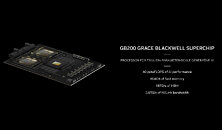
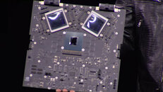
NVIDIA did not disclose the counts of the various SIMD components such as streaming multiprocessors per chiplet, CUDA cores, Tensor cores, or on-die cache sizes, but made performance claims. Each B200 chip provides 20 PFLOPs (that's 20,000 TFLOPs) of AI inferencing performance. "Blackwell" introduces NVIDIA's 2nd generation Transformer engine, and 6th generation Tensor core, which supports FP4 and FP6. The 5th Gen NVLink interface not just scales up within the node, but also scales out to up to 576 GPUs. Among NVIDIA's performance claims for the GB200 are 20 PFLOPs FP4 Tensor (dense), and 40 PFLOPs FP4 Tensor (sparse); 10 PFLOPs FP8 Tensor (dense); and 20 PFLOPs FP8 Tensor (sparse); 5 PFLOPs Bfloat16 and FP16 (10 PFLOPs with sparsity); and 2.5 PFLOPs TF32 Tensor (dense) with 5 PFLOPs (sparse). As a high-precision compute accelerator (FP64), the B200 provides 90 TFLOPs, which is a 3x increase over that of the GH200 "Hopper."
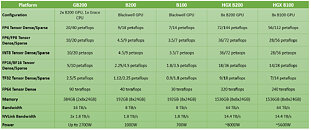
NVIDIA is expected to ship the B100, B200, and GB200, and their first-party derivatives, such as the SuperPODs, later this year.
View at TechPowerUp Main Site | Source
Each chiplet is built on the TSMC N4P foundry node, which is the most advanced 4 nm-class node by the Taiwanese foundry. Each chiplet has 104 billion transistors. The two chiplets have a high degree of connectivity with each other, thanks to a 10 TB/s custom interconnect. This is enough bandwidth and latency for the two to maintain cache coherency (i.e. address each other's memory as if they're their own). Each of the two "Blackwell" chiplets has a 4096-bit memory bus, and is wired to 96 GB of HBM3E spread across four 24 GB stacks; which totals to 192 GB for the B200 package. The GPU has a staggering 8 TB/s of memory bandwidth on tap. The B200 package features a 1.8 TB/s NVLink interface for host connectivity, and connectivity to another B200 chip.


NVIDIA also announced the Grace-Blackwell GB200 Superchip. This is a module that has two B200 GPUs wired to an NVIDIA Grace CPU that offers superior serial processing performance than x86-64 based CPUs from Intel or AMD; and an ISA that's highly optimized for NVIDIA's AI GPUs. The biggest advantage of the Grace CPU over an Intel Xeon Scalable or AMD EPYC has to be its higher bandwidth NVLink interconnect to the GPUs, compared to PCIe connections for x86-64 hosts. NVIDIA appears to be carrying over the Grace CPU from the GH200 Grace-Hopper Superchip.


NVIDIA did not disclose the counts of the various SIMD components such as streaming multiprocessors per chiplet, CUDA cores, Tensor cores, or on-die cache sizes, but made performance claims. Each B200 chip provides 20 PFLOPs (that's 20,000 TFLOPs) of AI inferencing performance. "Blackwell" introduces NVIDIA's 2nd generation Transformer engine, and 6th generation Tensor core, which supports FP4 and FP6. The 5th Gen NVLink interface not just scales up within the node, but also scales out to up to 576 GPUs. Among NVIDIA's performance claims for the GB200 are 20 PFLOPs FP4 Tensor (dense), and 40 PFLOPs FP4 Tensor (sparse); 10 PFLOPs FP8 Tensor (dense); and 20 PFLOPs FP8 Tensor (sparse); 5 PFLOPs Bfloat16 and FP16 (10 PFLOPs with sparsity); and 2.5 PFLOPs TF32 Tensor (dense) with 5 PFLOPs (sparse). As a high-precision compute accelerator (FP64), the B200 provides 90 TFLOPs, which is a 3x increase over that of the GH200 "Hopper."

NVIDIA is expected to ship the B100, B200, and GB200, and their first-party derivatives, such as the SuperPODs, later this year.
View at TechPowerUp Main Site | Source


