- Joined
- Aug 19, 2017
- Messages
- 2,929 (1.05/day)
According to Bloomberg's latest investigation, Huawei and Semiconductor Manufacturing International Corporation (SMIC) have submitted patents on the self-aligned quadruple patterning (SAQP) pattern etching technique to enable SMIC to achieve 5 nm semiconductor production. The two Chinese giants have been working with the Deep Ultra Violet (DUV) machinery to develop a pattern etching technique allowing SMIC to produce a node compliant with the US exporting rules while maintaining the density improvements from the previously announced 7 nm node. In the 7 nm process, SMIC most likely used self-aligned dual patterning (SADP) with DUV tools, but for the increased density of the 5 nm node, a doubling to SAQP is required. In semiconductor manufacturing, lithography tools take multiple turns to etch the design of the silicon wafer.
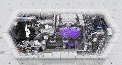
Especially with smaller nodes getting ever-increasing density requirements, it is becoming challenging to etch sub-10 nm designs using DUV tools. That is where Extreme Ultra Violet (EUV) tools from ASML come into play. With EUV, the wavelengths of the lithography printers are 14 times smaller than DUV, at only 13.5 nm, compared to 193 nm of ArF immersion DUV systems. This means that without EUV, SMIC has to look into alternatives like SAQP to increase the density of its nodes and, as a result, include more complications and possibly lower yields. As an example, Intel tried to use SAQP in its first 10 nm nodes to reduce reliance on EUV, which resulted in a series of delays and complications, eventually pushing Intel into EUV. While Huawei and SMIC may develop a more efficient solution for SAQP, the use of EUV is imminent as the regular DUV can not keep up with the increasing density of semiconductor nodes. Given that ASML can't ship its EUV machinery to China, Huawei is supposedly developing its own EUV machines, but will likely take a few more years to show.

View at TechPowerUp Main Site | Source
Especially with smaller nodes getting ever-increasing density requirements, it is becoming challenging to etch sub-10 nm designs using DUV tools. That is where Extreme Ultra Violet (EUV) tools from ASML come into play. With EUV, the wavelengths of the lithography printers are 14 times smaller than DUV, at only 13.5 nm, compared to 193 nm of ArF immersion DUV systems. This means that without EUV, SMIC has to look into alternatives like SAQP to increase the density of its nodes and, as a result, include more complications and possibly lower yields. As an example, Intel tried to use SAQP in its first 10 nm nodes to reduce reliance on EUV, which resulted in a series of delays and complications, eventually pushing Intel into EUV. While Huawei and SMIC may develop a more efficient solution for SAQP, the use of EUV is imminent as the regular DUV can not keep up with the increasing density of semiconductor nodes. Given that ASML can't ship its EUV machinery to China, Huawei is supposedly developing its own EUV machines, but will likely take a few more years to show.

View at TechPowerUp Main Site | Source


