- Joined
- Oct 9, 2007
- Messages
- 47,511 (7.49/day)
- Location
- Hyderabad, India
| System Name | RBMK-1000 |
|---|---|
| Processor | AMD Ryzen 7 5700G |
| Motherboard | ASUS ROG Strix B450-E Gaming |
| Cooling | DeepCool Gammax L240 V2 |
| Memory | 2x 8GB G.Skill Sniper X |
| Video Card(s) | Palit GeForce RTX 2080 SUPER GameRock |
| Storage | Western Digital Black NVMe 512GB |
| Display(s) | BenQ 1440p 60 Hz 27-inch |
| Case | Corsair Carbide 100R |
| Audio Device(s) | ASUS SupremeFX S1220A |
| Power Supply | Cooler Master MWE Gold 650W |
| Mouse | ASUS ROG Strix Impact |
| Keyboard | Gamdias Hermes E2 |
| Software | Windows 11 Pro |
Intel Core Ultra "Lunar Lake-MX" will be the company's bulwark against Apple's M-series Pro and Max chips, designed to power the next crop of performance ultraportables. The MX codename extension denotes MoP (memory-on-package), which sees stacked LPDDR5X memory chips share the package's fiberglass substrate with the chip, to conserve PCB footprint, and give Intel greater control over the right kind of memory speed, timings, and power-management features suited to its microarchitecture. This is essentially what Apple does with its M-series SoCs powering its MacBooks and iPad Pros. Igor's Lab scored the motherlode on the way Intel has restructured the various components across its chiplets, and the various I/O wired to the package.
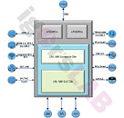
When compared to "Meteor Lake," the "Lunar Lake" microarchitecture sees a small amount of "re-aggregation" of the various logic-heavy components of the processor. On "Meteor Lake," the CPU cores and the iGPU sat on separate tiles—Compute tile and Graphics tile, respectively, with a large SoC tile sitting between them, and a smaller I/O tile that serves as an extension of the SoC tile. All four tiles sat on top of a Foveros base tile, which is essentially an interposer—a silicon die that facilitates high-density microscopic wiring between the various tiles that are placed on top of it. With "Lunar Lake," there are only two tiles—the Compute tile, and the SoC tile.


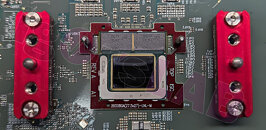
The Compute tile contains the CPU cores, and is built on the TSMC N3B foundry node. This is a 3 nm EUV node, and is said to be more advanced than the Intel 4 node that the company used for the Compute tile of "Meteor Lake." The processor pictured above features a 4P+4E CPU core configuration. That's four "Lion Cove" P-cores, and four "Skymont" E-cores. Considering that Intel used 2P+8E CPU core configurations in the 7 W and 15 W U-segments for "Alder Lake," "Lunar Lake-MX" is a step-up in terms of CPU performance, even if the CPU core count itself is down by 2. It's worth noting here, that the "Lion Cove" P-cores do not feature HTT, and so the logical processor count is 8.
At this point, it is not clear where the iGPU resides. On "Meteor Lake," the iGPU had its own tile called the Graphics tile, the processor's memory controllers were located on the SoC tile along with the NPU; and both the iGPU and CPU cores would rely on the SoC tile for memory access. An iGPU is as much a memory latency-sensitive device as an NPU, and so, one theory holds that the iGPU of "Lunar Lake" is located in the SoC tile along with the NPU, for the least possible latency to the memory controllers; the other less likely theory is that it's located on the 3 nm Compute tile.
This is because with Igor's confirmation that the Compute tile is built on TSMC N3B, and Intel Foundry slides mentioning the debut of the Intel 18A node with "Lunar Lake," it is the SoC tile that's built on Intel 18A. Logically, Intel 18A should be more advanced than TSMC N3B, since it incorporates nanosheet transistors, EUV lithography, and higher transistor densities. It hence makes more sense for Intel to leave the iGPU and NPU on the SoC tile, along with the memory controllers.
As for the iGPU itself, Igor's Lab confirms Intel's use of its next-generation Xe2-LPG "Battlemage" graphics architecture, which promises a generational leap in performance over Xe-LPG "Alchemist." The iGPU is expected to meet the full DirectX 12 Ultimate feature-set, as well as offer XeSS. The iGPU model on "Lunar Lake-MX" comes with 64 EU (execution units), and 8 Xe2 cores; although other variants of "Lunar Lake" could come with larger iGPUs.
Lastly, we move onto the bountiful I/O of "Lunar Lake-MX," starting with its LPDDR5X memory interface for on-package LPDDR5X-8533 memory. The package puts out both PCI-Express Gen 5 and Gen 4 lanes. The Gen 5 lanes are ideally meant for the chip's PEG interface, and a discrete GPU, and a Gen 5 NVMe SSD; while the Gen 4 lanes are meant to be general purpose—for secondary NVMe SSDs, or other onboard discrete devices. The processor has an integrated Wi-Fi 7 + Bluetooth 6 WLAN controller, and MACs for wired GbE controllers.
The main high-bandwidth connector from the "Lunar Lake-MX" is the chip's integrated Thunderbolt 4 interface, and USB4 interface, which can be configured by OEMs for power delivery. The chip also puts out regular USB 3.2 and USB 2.0 connectivity. Display connectivity includes DisplayPort 2.1, HDMI 2.1, and eDP 1.5. The DisplayPort 2.1 can be multiplexed with USB-C ports.
View at TechPowerUp Main Site | Source
When compared to "Meteor Lake," the "Lunar Lake" microarchitecture sees a small amount of "re-aggregation" of the various logic-heavy components of the processor. On "Meteor Lake," the CPU cores and the iGPU sat on separate tiles—Compute tile and Graphics tile, respectively, with a large SoC tile sitting between them, and a smaller I/O tile that serves as an extension of the SoC tile. All four tiles sat on top of a Foveros base tile, which is essentially an interposer—a silicon die that facilitates high-density microscopic wiring between the various tiles that are placed on top of it. With "Lunar Lake," there are only two tiles—the Compute tile, and the SoC tile.


The Compute tile contains the CPU cores, and is built on the TSMC N3B foundry node. This is a 3 nm EUV node, and is said to be more advanced than the Intel 4 node that the company used for the Compute tile of "Meteor Lake." The processor pictured above features a 4P+4E CPU core configuration. That's four "Lion Cove" P-cores, and four "Skymont" E-cores. Considering that Intel used 2P+8E CPU core configurations in the 7 W and 15 W U-segments for "Alder Lake," "Lunar Lake-MX" is a step-up in terms of CPU performance, even if the CPU core count itself is down by 2. It's worth noting here, that the "Lion Cove" P-cores do not feature HTT, and so the logical processor count is 8.
At this point, it is not clear where the iGPU resides. On "Meteor Lake," the iGPU had its own tile called the Graphics tile, the processor's memory controllers were located on the SoC tile along with the NPU; and both the iGPU and CPU cores would rely on the SoC tile for memory access. An iGPU is as much a memory latency-sensitive device as an NPU, and so, one theory holds that the iGPU of "Lunar Lake" is located in the SoC tile along with the NPU, for the least possible latency to the memory controllers; the other less likely theory is that it's located on the 3 nm Compute tile.
This is because with Igor's confirmation that the Compute tile is built on TSMC N3B, and Intel Foundry slides mentioning the debut of the Intel 18A node with "Lunar Lake," it is the SoC tile that's built on Intel 18A. Logically, Intel 18A should be more advanced than TSMC N3B, since it incorporates nanosheet transistors, EUV lithography, and higher transistor densities. It hence makes more sense for Intel to leave the iGPU and NPU on the SoC tile, along with the memory controllers.
As for the iGPU itself, Igor's Lab confirms Intel's use of its next-generation Xe2-LPG "Battlemage" graphics architecture, which promises a generational leap in performance over Xe-LPG "Alchemist." The iGPU is expected to meet the full DirectX 12 Ultimate feature-set, as well as offer XeSS. The iGPU model on "Lunar Lake-MX" comes with 64 EU (execution units), and 8 Xe2 cores; although other variants of "Lunar Lake" could come with larger iGPUs.
Lastly, we move onto the bountiful I/O of "Lunar Lake-MX," starting with its LPDDR5X memory interface for on-package LPDDR5X-8533 memory. The package puts out both PCI-Express Gen 5 and Gen 4 lanes. The Gen 5 lanes are ideally meant for the chip's PEG interface, and a discrete GPU, and a Gen 5 NVMe SSD; while the Gen 4 lanes are meant to be general purpose—for secondary NVMe SSDs, or other onboard discrete devices. The processor has an integrated Wi-Fi 7 + Bluetooth 6 WLAN controller, and MACs for wired GbE controllers.
The main high-bandwidth connector from the "Lunar Lake-MX" is the chip's integrated Thunderbolt 4 interface, and USB4 interface, which can be configured by OEMs for power delivery. The chip also puts out regular USB 3.2 and USB 2.0 connectivity. Display connectivity includes DisplayPort 2.1, HDMI 2.1, and eDP 1.5. The DisplayPort 2.1 can be multiplexed with USB-C ports.
View at TechPowerUp Main Site | Source


