- Joined
- May 21, 2024
- Messages
- 1,143 (3.48/day)
PanelSemi, a developer of ultra-thin flexible LED displays and semiconductor substrates, has partnered with NGK Insulators to create high-performance hybrid packaging solutions. Leveraging its tiled thin-film transistor (TFT) circuit fabrication technology, PanelSemi is developing a hybrid circuit board that combines fine wiring and functional circuits on polyimide film with a ceramic substrate. The company is expanding into high-performance circuit boards for semiconductor modules, targeting large-scale panel manufacturing for wireless communications and opto-electronic integration. The collaboration with NGK extends the application of ceramic substrates to higher power and thermal scenarios.
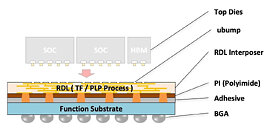
NGK aims to integrate PanelSemi's circuit fabrication technology with its own products, including the ultra-compact EnerCera lithium-ion rechargeable battery, ceramic substrates, and ceramic packages. PanelSemi's HyBrid Substrate (HBS) technology platform features ultra-fine line width and spacing achieved through Thin Film (TF) and Panel Level Packaging (PLP) processes. HBS enables high-density interconnection, functioning as both an interposer and package substrate in advanced packaging, with the top die directly bonded to the HBS.

View at TechPowerUp Main Site | Source
NGK aims to integrate PanelSemi's circuit fabrication technology with its own products, including the ultra-compact EnerCera lithium-ion rechargeable battery, ceramic substrates, and ceramic packages. PanelSemi's HyBrid Substrate (HBS) technology platform features ultra-fine line width and spacing achieved through Thin Film (TF) and Panel Level Packaging (PLP) processes. HBS enables high-density interconnection, functioning as both an interposer and package substrate in advanced packaging, with the top die directly bonded to the HBS.

View at TechPowerUp Main Site | Source

