- Joined
- Oct 9, 2007
- Messages
- 47,638 (7.44/day)
- Location
- Dublin, Ireland
| System Name | RBMK-1000 |
|---|---|
| Processor | AMD Ryzen 7 5700G |
| Motherboard | Gigabyte B550 AORUS Elite V2 |
| Cooling | DeepCool Gammax L240 V2 |
| Memory | 2x 16GB DDR4-3200 |
| Video Card(s) | Galax RTX 4070 Ti EX |
| Storage | Samsung 990 1TB |
| Display(s) | BenQ 1440p 60 Hz 27-inch |
| Case | Corsair Carbide 100R |
| Audio Device(s) | ASUS SupremeFX S1220A |
| Power Supply | Cooler Master MWE Gold 650W |
| Mouse | ASUS ROG Strix Impact |
| Keyboard | Gamdias Hermes E2 |
| Software | Windows 11 Pro |
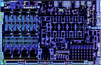
The first die shot of AMD's new 4 nm "Strix Point" mobile processor surfaced, thanks to an enthusiast on Chinese social media. "Strix Point" is a significantly larger die than "Phoenix." It measures 12.06 mm x 18.71 mm (L x W), compared to the 9.06 mm x 15.01 mm of "Phoenix." Much of this die size increase comes from the larger CPU, iGPU, and NPU. The process has been improved from TSMC N4 on "Phoenix" and its derivative "Hawk Point," to the newer TSMC N4P node.
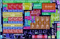
Nemez (GPUsAreMagic) annotated the die shot in great detail. The CPU now has 12 cores spread across two CCX, one of which contains four "Zen 5" cores sharing a 16 MB L3 cache; and the other with eight "Zen 5c" cores sharing an 8 MB L3 cache. The two CCXs connect to the rest of the chip over Infinity Fabric. The rather large iGPU takes up the central region of the die. It is based on the RDNA 3.5 graphics architecture, and features 8 workgroup processors (WGPs), or 16 compute units (CU) worth 1,024 stream processors. Other key components include four render backends worth 16 ROPs, and control logic. The GPU has its own 2 MB of L2 cache that cushions transfers to the Infinity Fabric.


Slightly separated from the iGPU are its allied components, the Media Engine, and the Display Engine. The Media Engine provides hardware acceleration for encoding and decoding of h.264, h.265, and AV1, besides several legacy video formats. The Display Engine is responsible for encoding the frame output of the iGPU to the various connector formats (such as DisplayPort, eDP, HDMI), including hardware-accelerated display stream compression; while the display PHYs handle the physical layer of the connectors.
The NPU is the third major logic component of "Strix Point." This second generation NPU by AMD is visibly larger than the one found in "Phoenix." It is based on the more advanced XDNA 2 architecture, and contains 32 AI engine tiles, talking to its own high-speed local memory, and a control logic that interfaces with Infinity Fabric. This NPU is designed to meet and exceed the hardware requirements of Microsoft Copilot+, and provides a throughput of 50 TOPS.
The memory controller supports dual-channel (160-bit) DDR5 with native DDR5-5600; and 128-bit LPDDR5 at speeds of up to LPDDR5-7500. The controller features an unspecified size of SRAM cache, which Nemez notes was also seen on the "Phoenix 2" and "Phoenix" dies, but not on the memory controller of the cIOD found in "Raphael" and "Dragon Range."
The "Strix Point" silicon has a smaller PCIe root complex than "Phoenix," which in turn has a smaller root complex than "Cezanne." AMD has been reducing the PCIe lane count by 4 over the past three generations. "Cezanne" features 24 PCIe Gen 3 lanes (x16 PEG + x4 NVMe + x4 chipset bus or GPP); while "Phoenix" truncates this to 20 PCIe Gen 4 lanes (x8 PEG + x4 NVMe + x4 chipset bus or GPP + x4 configured as USB4). The newer "Strix Point" cuts it down further to just 16 PCIe Gen 4 lanes (x8 PEG + x4 NVMe + x4 configured as USB4 or GPP).
The idea behind the PCIe lane reduction is that "Strix Point" is designed to square off against "Lunar Lake," which too only has x4 for PEG/GPP, and when "Arrow Lake-H" and "Arrow Lake-HX" eventually hit the scene, they'll be met with AMD's "Fire Range" chip that has a 28-lane PCIe Gen 5 interface and can be paired with even the fastest discrete mobile GPUs.
View at TechPowerUp Main Site | Source
Nemez (GPUsAreMagic) annotated the die shot in great detail. The CPU now has 12 cores spread across two CCX, one of which contains four "Zen 5" cores sharing a 16 MB L3 cache; and the other with eight "Zen 5c" cores sharing an 8 MB L3 cache. The two CCXs connect to the rest of the chip over Infinity Fabric. The rather large iGPU takes up the central region of the die. It is based on the RDNA 3.5 graphics architecture, and features 8 workgroup processors (WGPs), or 16 compute units (CU) worth 1,024 stream processors. Other key components include four render backends worth 16 ROPs, and control logic. The GPU has its own 2 MB of L2 cache that cushions transfers to the Infinity Fabric.


Slightly separated from the iGPU are its allied components, the Media Engine, and the Display Engine. The Media Engine provides hardware acceleration for encoding and decoding of h.264, h.265, and AV1, besides several legacy video formats. The Display Engine is responsible for encoding the frame output of the iGPU to the various connector formats (such as DisplayPort, eDP, HDMI), including hardware-accelerated display stream compression; while the display PHYs handle the physical layer of the connectors.
The NPU is the third major logic component of "Strix Point." This second generation NPU by AMD is visibly larger than the one found in "Phoenix." It is based on the more advanced XDNA 2 architecture, and contains 32 AI engine tiles, talking to its own high-speed local memory, and a control logic that interfaces with Infinity Fabric. This NPU is designed to meet and exceed the hardware requirements of Microsoft Copilot+, and provides a throughput of 50 TOPS.
The memory controller supports dual-channel (160-bit) DDR5 with native DDR5-5600; and 128-bit LPDDR5 at speeds of up to LPDDR5-7500. The controller features an unspecified size of SRAM cache, which Nemez notes was also seen on the "Phoenix 2" and "Phoenix" dies, but not on the memory controller of the cIOD found in "Raphael" and "Dragon Range."
The "Strix Point" silicon has a smaller PCIe root complex than "Phoenix," which in turn has a smaller root complex than "Cezanne." AMD has been reducing the PCIe lane count by 4 over the past three generations. "Cezanne" features 24 PCIe Gen 3 lanes (x16 PEG + x4 NVMe + x4 chipset bus or GPP); while "Phoenix" truncates this to 20 PCIe Gen 4 lanes (x8 PEG + x4 NVMe + x4 chipset bus or GPP + x4 configured as USB4). The newer "Strix Point" cuts it down further to just 16 PCIe Gen 4 lanes (x8 PEG + x4 NVMe + x4 configured as USB4 or GPP).
The idea behind the PCIe lane reduction is that "Strix Point" is designed to square off against "Lunar Lake," which too only has x4 for PEG/GPP, and when "Arrow Lake-H" and "Arrow Lake-HX" eventually hit the scene, they'll be met with AMD's "Fire Range" chip that has a 28-lane PCIe Gen 5 interface and can be paired with even the fastest discrete mobile GPUs.
View at TechPowerUp Main Site | Source


