- Joined
- May 21, 2024
- Messages
- 1,497 (3.58/day)
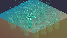
Lam Research Corp. today extended its leadership in 3D NAND flash memory etching with the introduction of Lam Cryo 3.0, the third generation of the company's production-proven cryogenic dielectric etch technology. As the proliferation of generative artificial intelligence (AI) continues to propel the demand for memory with higher capacity and performance, Lam Cryo 3.0 provides etch capabilities critical for the manufacturing of future leading-edge 3D NAND. Leveraging ultra cold temperatures, high power confined plasma reactor technology, and innovations in surface chemistry, Lam Cryo 3.0 etches with industry-leading precision and profile control.
"Lam Cryo 3.0 paves the way for customers on the path to 1,000-layer 3D NAND," said Sesha Varadarajan, senior vice president of Global Products Group at Lam Research. "With five million wafers already manufactured using Lam cryogenic etch, our newest technology is a breakthrough in 3D NAND production. It creates high aspect ratio (HAR) features with angstrom-level precision, while delivering lower environmental impact and more than double the etch rate of conventional dielectric processes. Lam Cryo 3.0 is the etch technology our customers need to overcome the AI era's key NAND manufacturing hurdles."
To date, 3D NAND has primarily advanced through the stacking of vertical layers of memory cells, which are enabled by etching deep and narrow HAR memory channels. Slight, atomic-scale deviations from the target profile of these features can negatively affect electrical properties of the die and potentially impact yield. Lam Cryo 3.0 is optimized to address these and other etch challenges to scaling.
The Industry's Most Advanced Cryogenic Etch Technology
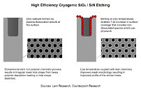
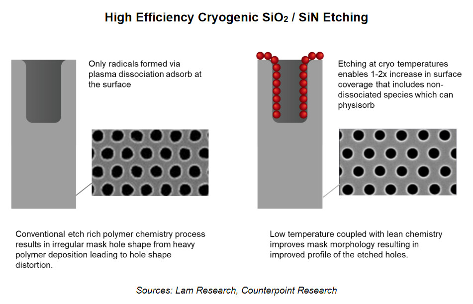
Lam Cryo 3.0 utilizes the company's unique, high powered confined plasma reactors, process improvements and temperatures well below -0°C, which permit the harnessing of new, novel etch chemistries. When combined with the scalable, pulsed plasma technology of Lam's latest Vantex dielectric system, etch depth and profile control is significantly increased. Using Lam Cryo 3.0 technology, 3D NAND manufacturers can etch memory channels with depths of up to 10 microns with less than 0.1% deviation in the feature's critical dimension from the top to the bottom.
Other highlights include:
Leading 3D NAND Dielectric Etching
Lam Cryo 3.0 further extends to the company's two-decade-leadership in wafer fabrication etch technologies, which includes seven generations of 3D NAND. Lam introduced the world's first cryogenic etch offering into volume production in 2019. Of the over 7,500 Lam HAR dielectric etch chambers utilized in NAND production today, nearly 1,000 of them use cryogenic etch technology.
Lam Cryo 3.0 is now available to leading memory manufacturers. It is the latest addition to Lam's broad portfolio of etch, deposition and clean solutions for 3D NAND manufacturing.
View at TechPowerUp Main Site | Source
"Lam Cryo 3.0 paves the way for customers on the path to 1,000-layer 3D NAND," said Sesha Varadarajan, senior vice president of Global Products Group at Lam Research. "With five million wafers already manufactured using Lam cryogenic etch, our newest technology is a breakthrough in 3D NAND production. It creates high aspect ratio (HAR) features with angstrom-level precision, while delivering lower environmental impact and more than double the etch rate of conventional dielectric processes. Lam Cryo 3.0 is the etch technology our customers need to overcome the AI era's key NAND manufacturing hurdles."


To date, 3D NAND has primarily advanced through the stacking of vertical layers of memory cells, which are enabled by etching deep and narrow HAR memory channels. Slight, atomic-scale deviations from the target profile of these features can negatively affect electrical properties of the die and potentially impact yield. Lam Cryo 3.0 is optimized to address these and other etch challenges to scaling.
"AI is driving exponential demand in capacity and on the performance of flash memory both at the cloud and the edge. This is compelling chipmakers to scale NAND flash in the race to achieve 1000-layer 3D NAND by the end of 2030," said Neil Shah, co-founder and vice president of research at Counterpoint Research. "Lam Cryo 3.0 cryogenic etch technology is a significant leap beyond conventional techniques. It etches memory channels that are more than 50 times deeper than their width with near perfect precision and control, achieving a profile deviation of less than 0.1%. This breakthrough significantly enhances advanced 3D NAND yields and overall performance to enable chipmakers to compete well in the AI era."
The Industry's Most Advanced Cryogenic Etch Technology
Lam Cryo 3.0 utilizes the company's unique, high powered confined plasma reactors, process improvements and temperatures well below -0°C, which permit the harnessing of new, novel etch chemistries. When combined with the scalable, pulsed plasma technology of Lam's latest Vantex dielectric system, etch depth and profile control is significantly increased. Using Lam Cryo 3.0 technology, 3D NAND manufacturers can etch memory channels with depths of up to 10 microns with less than 0.1% deviation in the feature's critical dimension from the top to the bottom.
Other highlights include:
- Outstanding Productivity: Compared to conventional dielectric processes, Lam Cryo 3.0 etches two-and-a-half times faster, with better wafer-to-wafer repeatability, helping 3D NAND manufacturers to achieve high yield at lower cost.
- Higher Sustainability: Lam Cryo offers 40% reduction in energy consumption per wafer, and up to a 90% reduction in emissions compared to conventional etch processes.
- Maximize Equipment Investment: For the optimal profile control and the fastest and deepest dielectric etch, Lam Cryo 3.0 can be integrated into Lam's newest Vantex system. It is also compatible with the company's portfolio of Flex HAR dielectric etchers, used by all major memory manufacturers for 3D NAND mass production.
Leading 3D NAND Dielectric Etching
Lam Cryo 3.0 further extends to the company's two-decade-leadership in wafer fabrication etch technologies, which includes seven generations of 3D NAND. Lam introduced the world's first cryogenic etch offering into volume production in 2019. Of the over 7,500 Lam HAR dielectric etch chambers utilized in NAND production today, nearly 1,000 of them use cryogenic etch technology.
Lam Cryo 3.0 is now available to leading memory manufacturers. It is the latest addition to Lam's broad portfolio of etch, deposition and clean solutions for 3D NAND manufacturing.
View at TechPowerUp Main Site | Source


