- Joined
- May 21, 2024
- Messages
- 1,109 (3.53/day)
SK hynix is reportedly developing 400-layer NAND flash memory, with plans to begin mass production by late 2025. The company is collaborating with supply chain partners to develop the necessary process technologies and equipment for 400-layer and higher NAND chips. This information comes from a recent article by Korean media outlet etnews citing industry sources.
SK hynix intends to use hybrid bonding technology to achieve this, which is expected to bring new packaging materials and components suppliers into the supply chain. The development process involves exploring new bonding materials and various technologies for connecting different wafers, including polishing, etching, deposition, and wiring. SK hynix aims to have the technology and infrastructure ready by the end of next year.

This trend of increasing NAND chip layers is not unique to SK hynix; other semiconductor manufacturers are pushing in the same direction:
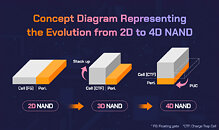
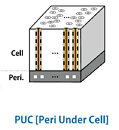
In comparison, SK hynix showcased a 321-layer NAND sample in August 2023. To reach 400 layers, the company plans to implement hybrid bonding with a "wafer-to-wafer" (W2W) structure. This approach differs from their current "Peripheral Under Cell" (PUC) method, which stacks cells atop the peripheral driving circuit area.
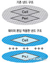
The shift to hybrid bonding aims to address challenges with increasing layer counts, such as potential damage to peripherals during the cell stacking process due to high heat and pressure. By manufacturing cells and peripherals on separate wafers before bonding them, SK hynix hopes to enable stable layer increases while protecting the peripheral components.
When asked by etnews about the 400-layer NAND development, SK hynix declined to confirm specific details regarding the technology development or mass production timelines.
View at TechPowerUp Main Site | Source
SK hynix intends to use hybrid bonding technology to achieve this, which is expected to bring new packaging materials and components suppliers into the supply chain. The development process involves exploring new bonding materials and various technologies for connecting different wafers, including polishing, etching, deposition, and wiring. SK hynix aims to have the technology and infrastructure ready by the end of next year.


This trend of increasing NAND chip layers is not unique to SK hynix; other semiconductor manufacturers are pushing in the same direction:
- Samsung recently began mass production of 290-layer V-NAND and aims for over 1000 layers by 2030
- Micron launched a product using 276-layer 3D NAND in July
- Kioxia achieved 218 layers in 2023 and suggests 1000 layers may be possible by 2027
In comparison, SK hynix showcased a 321-layer NAND sample in August 2023. To reach 400 layers, the company plans to implement hybrid bonding with a "wafer-to-wafer" (W2W) structure. This approach differs from their current "Peripheral Under Cell" (PUC) method, which stacks cells atop the peripheral driving circuit area.
The shift to hybrid bonding aims to address challenges with increasing layer counts, such as potential damage to peripherals during the cell stacking process due to high heat and pressure. By manufacturing cells and peripherals on separate wafers before bonding them, SK hynix hopes to enable stable layer increases while protecting the peripheral components.
When asked by etnews about the 400-layer NAND development, SK hynix declined to confirm specific details regarding the technology development or mass production timelines.
View at TechPowerUp Main Site | Source


