• Welcome to TechPowerUp Forums, Guest! Please check out our forum guidelines for info related to our community.

Coalition Formed to Accelerate the Use of Glass Substrates for Advanced Chips and Chiplets

Nomad76

News Editor
Staff member
Joined
May 21, 2024
Messages
536 (3.75/day)
E&R Engineering Corp. hosted an event on August 28, 2024, in Taipei, Taiwan, where they launched the "E-Core System." This initiative, a combination of "E&R" and "Glass Core" inspired by the sound of "Ecosystem," led to the establishment of the "Glass Substrate Supplier E-Core System Alliance." The alliance aims to combine expertise to promote comprehensive solutions, providing equipment and materials for next-generation advanced packaging with glass substrates to both domestic and international customers.

E&R's E-Core Alliance includes Manz AG, Scientech for wet etching, HYAWEI OPTRONICS for AOI optical inspection, Lincotec, STK Corp., Skytech, Group Up for sputtering and ABF lamination equipment, and other key component suppliers such as HIWIN, HIWIN MIKROSYSTEM, Keyence Taiwan, Mirle Group, ACE PILLAR CHYI DING), and Coherent.


E&R will continue leading the development of glass substrate technology in Taiwan, optimizing processes, and collaborating with more industry partners to achieve excellence.

With the rapid growth in demand for AI chips, high-frequency, and high-speed communication devices, glass substrates in advanced packaging technologies are becoming increasingly important. Compared to the widespread use of copper foil substrates, glass substrates offer higher wiring density and better signal performance. Additionally, glass provides extremely high flatness and can withstand high temperatures and voltages, making it an ideal replacement for traditional substrates.

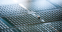
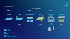
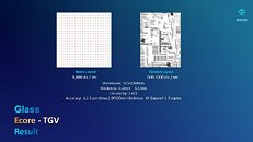
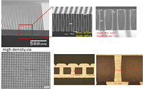
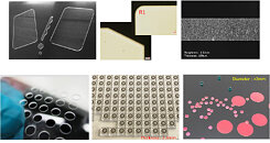
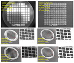
The glass substrate process involves glass metallization, the subsequent ABF (Ajinomoto Build-up Film) lamination, and final substrate cutting. Key steps in glass metallization include TGV (Through-Glass Via), wet etching, AOI (Automated Optical Inspection), sputtering, and plating. These glass substrates measure 515×510 mm, representing a new process in semiconductor and substrate manufacturing.

The critical aspect of glass substrate technology is the first step—glass laser modification (TGV). Although introduced over a decade ago, its speed had not met mass production requirements, achieving only 10 to 50 vias per second, limiting the market impact of glass substrates. E&R Engineering Corp has been working with a North American IDM customer for the past five years to develop glass laser modification TGV technology. Last year, the process passed validation, with E&R mastering key technology, now achieving up to 8,000 vias per second for fixed patterns (matrix layouts) or 600 to 1,000 vias per second for customized patterns (random layouts), with an accuracy of +/- 5 μm, meeting the 3 sigma standard. This breakthrough has finally enabled glass substrates to reach mass production.


View at TechPowerUp Main Site | Source
 
Joined
Jan 3, 2021
Messages
3,342 (2.43/day)
Location
Slovenia
Processor i5-6600K
Motherboard Asus Z170A
Cooling some cheap Cooler Master Hyper 103 or similar
Memory 16GB DDR4-2400
Video Card(s) IGP
Storage Samsung 850 EVO 250GB
Display(s) 2x Oldell 24" 1920x1200
Case Bitfenix Nova white windowless non-mesh
Audio Device(s) E-mu 1212m PCI
Power Supply Seasonic G-360
Mouse Logitech Marble trackball, never had a mouse
Keyboard Key Tronic KT2000, no Win key because 1994
Software Oldwin
What's the advantage of glass substrates/interposers over those made of silicon?

I can only see disadvantages: different thermal expansion between silicon chips and the glass substrate, and low thermal conductivity of glass. But that's just a general remark because many different types of glass exist.
 
Joined
Aug 18, 2022
Messages
359 (0.46/day)
What's the advantage of glass substrates/interposers over those made of silicon?
There is a mention that "...E&R Engineering Corp has been working with a North American IDM customer for the past five years to develop glass laser modification TGV technology..." - this customer is Intel.

See the image below of what Intel claim are the advantages of glass core substrates.

Glass Core Substrate Presentation Deck_6.png
 
Joined
Jan 29, 2012
Messages
6,845 (1.48/day)
Location
Florida
System Name natr0n-PC
Processor Ryzen 5950x-5600x | 9600k
Motherboard B450 AORUS M | Z390 UD
Cooling EK AIO 360 - 6 fan action | AIO
Memory Patriot - Viper Steel DDR4 (B-Die)(4x8GB) | Samsung DDR4 (4x8GB)
Video Card(s) EVGA 3070ti FTW
Storage Various
Display(s) Pixio PX279 Prime
Case Thermaltake Level 20 VT | Black bench
Audio Device(s) LOXJIE D10 + Kinter Amp + 6 Bookshelf Speakers Sony+JVC+Sony
Power Supply Super Flower Leadex III ARGB 80+ Gold 650W | EVGA 700 Gold
Software XP/7/8.1/10
Benchmark Scores http://valid.x86.fr/79kuh6
maybe less wasted parts cause glass can be remelted infinitely
 
Joined
Jan 11, 2022
Messages
768 (0.76/day)
maybe less wasted parts cause glass can be remelted infinitely
It needs the right properties to be suitable for certain jobs.
i doubt glass used for this can be used a second time as repeating introduces materials that change properties
 
Joined
Jan 29, 2012
Messages
6,845 (1.48/day)
Location
Florida
System Name natr0n-PC
Processor Ryzen 5950x-5600x | 9600k
Motherboard B450 AORUS M | Z390 UD
Cooling EK AIO 360 - 6 fan action | AIO
Memory Patriot - Viper Steel DDR4 (B-Die)(4x8GB) | Samsung DDR4 (4x8GB)
Video Card(s) EVGA 3070ti FTW
Storage Various
Display(s) Pixio PX279 Prime
Case Thermaltake Level 20 VT | Black bench
Audio Device(s) LOXJIE D10 + Kinter Amp + 6 Bookshelf Speakers Sony+JVC+Sony
Power Supply Super Flower Leadex III ARGB 80+ Gold 650W | EVGA 700 Gold
Software XP/7/8.1/10
Benchmark Scores http://valid.x86.fr/79kuh6
It needs the right properties to be suitable for certain jobs.
i doubt glass used for this can be used a second time as repeating introduces materials that change properties
indeed but they can send the glass waste to a recycle plant/glassware maker or something so no waste.
 
Joined
Aug 13, 2020
Messages
170 (0.11/day)
Is there really a practical consumer grade application for this? Glass circuit boards? It's bad enough that we have phones with the front & back being glass...I mean how many times does that break... now they're going to put glass in the phone/laptop? Sounds like a pretty risky idea unless this glass is somewhat flexible or super strong... I think there needs to be better messaging in order to communicate the advantages since I haven't seen advantages yet...
 
Joined
Dec 12, 2016
Messages
1,700 (0.59/day)
What's the advantage of glass substrates/interposers over those made of silicon?

I can only see disadvantages: different thermal expansion between silicon chips and the glass substrate, and low thermal conductivity of glass. But that's just a general remark because many different types of glass exist.
I don’t think the substrates are made of silicon. They are called Organic and make up the PCB of a CPU.
 
Joined
May 3, 2018
Messages
2,846 (1.21/day)
What's the advantage of glass substrates/interposers over those made of silicon?

I can only see disadvantages: different thermal expansion between silicon chips and the glass substrate, and low thermal conductivity of glass. But that's just a general remark because many different types of glass exist.


Why glass substrates
 
Joined
Sep 27, 2008
Messages
1,180 (0.20/day)
indeed but they can send the glass waste to a recycle plant/glassware maker or something so no waste.
That'll only happen if it's economically feasible to separate the materials for recycling. It's not so much a "glass substrate" as it is a "composite substrate containing glass"
 
Joined
Jan 3, 2021
Messages
3,342 (2.43/day)
Location
Slovenia
Processor i5-6600K
Motherboard Asus Z170A
Cooling some cheap Cooler Master Hyper 103 or similar
Memory 16GB DDR4-2400
Video Card(s) IGP
Storage Samsung 850 EVO 250GB
Display(s) 2x Oldell 24" 1920x1200
Case Bitfenix Nova white windowless non-mesh
Audio Device(s) E-mu 1212m PCI
Power Supply Seasonic G-360
Mouse Logitech Marble trackball, never had a mouse
Keyboard Key Tronic KT2000, no Win key because 1994
Software Oldwin
That'll only happen if it's economically feasible to separate the materials for recycling. It's not so much a "glass substrate" as it is a "composite substrate containing glass"
Will read, thanks. Fig. 1 already tells a lot about economics, even if the substrates in the illustration are only about 30 x 30 mm. Manufacturers have plans to develop much larger ones, which means that the space on a 300 mm round wafer would be used very inefficiently.
 
Joined
May 3, 2018
Messages
2,846 (1.21/day)
That'll only happen if it's economically feasible to separate the materials for recycling. It's not so much a "glass substrate" as it is a "composite substrate containing glass"
Nope it's pretty much glass glass. It might contain trace elements of other materials to achieve desired properties, not the other way around.
 
Joined
Jan 3, 2021
Messages
3,342 (2.43/day)
Location
Slovenia
Processor i5-6600K
Motherboard Asus Z170A
Cooling some cheap Cooler Master Hyper 103 or similar
Memory 16GB DDR4-2400
Video Card(s) IGP
Storage Samsung 850 EVO 250GB
Display(s) 2x Oldell 24" 1920x1200
Case Bitfenix Nova white windowless non-mesh
Audio Device(s) E-mu 1212m PCI
Power Supply Seasonic G-360
Mouse Logitech Marble trackball, never had a mouse
Keyboard Key Tronic KT2000, no Win key because 1994
Software Oldwin
Nope it's pretty much glass glass. It might contain trace elements of other materials to achieve desired properties, not the other way around.
Glass is the base material but a working substrate has layers of coper and insulation on it, which is either plastic film or some oxide or something similar. Those will may make up a significant part of substrate by weight and volume - my guess would be a couple tenths of a millimetre on each side of a ~1 mm thick glass. That won't be trivial to recycle.

But compared to glass fibre-reinforced resin, nearly everything else must be a child's game to recycle...
 
Top