- Joined
- Oct 9, 2007
- Messages
- 47,655 (7.44/day)
- Location
- Dublin, Ireland
| System Name | RBMK-1000 |
|---|---|
| Processor | AMD Ryzen 7 5700G |
| Motherboard | Gigabyte B550 AORUS Elite V2 |
| Cooling | DeepCool Gammax L240 V2 |
| Memory | 2x 16GB DDR4-3200 |
| Video Card(s) | Galax RTX 4070 Ti EX |
| Storage | Samsung 990 1TB |
| Display(s) | BenQ 1440p 60 Hz 27-inch |
| Case | Corsair Carbide 100R |
| Audio Device(s) | ASUS SupremeFX S1220A |
| Power Supply | Cooler Master MWE Gold 650W |
| Mouse | ASUS ROG Strix Impact |
| Keyboard | Gamdias Hermes E2 |
| Software | Windows 11 Pro |
As Intel's Core Ultra "Arrow Lake-S" desktop processors near their launch, ASUS China put out a video presentation about its Z890 chipset motherboards ready for these processors, which included a technical run-down of Intel's first tile-based desktop processor, which included detailed die-shots of the various tiles. This is stuff that would require not just de-lidding the processor (removing the integrated heat-spreader), but also clearing up the top layers of the die to reveal the various components underneath.
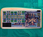
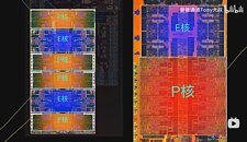
The whole-chip die-shot gives us a bird's eye view of the four key logic tiles—Compute, Graphics, SoC, and I/O, sitting on top of the Foveros base tile. Our article from earlier this week goes into the die areas of the individual tiles, and the base tile. The Compute tile is built on the most advanced foundry node among the four tiles, the 3 nm TSMC N3B. Unlike the older generation "Raptor Lake-S" and "Alder Lake-S," the P-cores and E-core clusters aren't clumped into the two ends of the CPU complex. In "Arrow Lake-S," they follow a staggered layout, with a row of P-cores, followed by a row of E-core clusters, followed by two rows of P-cores, and then another row of E-core clusters, before the final row of P-cores, to achieve the total core-count of 8P+16E. This arrangement reduces concentration of heat when the P-cores are loaded (eg: when gaming), and ensures each E-core cluster is just one ringbus stop away from a P-core, which should improve thread-migration latencies. The central region of the tile has this ringbus, and 36 MB of L3 cache shared among the P-cores and E-core clusters.
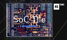
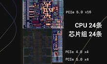
Next up, is the SoC tile. This chiplet is built on the 6 nm DUV TSMC N6 node. Both edges of the tile has PHYs for the various I/O interfaces. One side has the dual-channel DDR5 PHY, while the other has a portion of the chip's PCI-Express PHY. The SoC tile puts out 16 PCIe Gen 5 lanes meant for the PEG interface (the x16 slot on your motherboard). The I/O tile puts out four PCIe Gen 5 lanes, and four PCIe Gen 4 lanes, besides the DMI 4.0 x8 chipset bus. The Gen 4 x4 from the I/O can be reconfigured as Thunderbolt 4 or USB4. The SoC tile also contains the NPU 3 unit, which appears to be carried over from the SoC tile of "Meteor Lake." It has a peak throughput of 13 AI TOPS. The SoC tile also contains the chip's platform security processors, and a few allied components of the iGPU, namely the display engine, the media accelerators, and the display I/O.
Lastly, there's the Graphics tile. Intel built this on the fairly advanced 5 nm TSMC N5 process (same one that current NVIDIA Ada and AMD RDNA 3 GPUs are built on). This slender tile only contains the 4 Xe cores available to this iGPU variant, and graphics rendering machinery.
The filler tiles appear like voids under the microscope.
View at TechPowerUp Main Site | Source
The whole-chip die-shot gives us a bird's eye view of the four key logic tiles—Compute, Graphics, SoC, and I/O, sitting on top of the Foveros base tile. Our article from earlier this week goes into the die areas of the individual tiles, and the base tile. The Compute tile is built on the most advanced foundry node among the four tiles, the 3 nm TSMC N3B. Unlike the older generation "Raptor Lake-S" and "Alder Lake-S," the P-cores and E-core clusters aren't clumped into the two ends of the CPU complex. In "Arrow Lake-S," they follow a staggered layout, with a row of P-cores, followed by a row of E-core clusters, followed by two rows of P-cores, and then another row of E-core clusters, before the final row of P-cores, to achieve the total core-count of 8P+16E. This arrangement reduces concentration of heat when the P-cores are loaded (eg: when gaming), and ensures each E-core cluster is just one ringbus stop away from a P-core, which should improve thread-migration latencies. The central region of the tile has this ringbus, and 36 MB of L3 cache shared among the P-cores and E-core clusters.


Next up, is the SoC tile. This chiplet is built on the 6 nm DUV TSMC N6 node. Both edges of the tile has PHYs for the various I/O interfaces. One side has the dual-channel DDR5 PHY, while the other has a portion of the chip's PCI-Express PHY. The SoC tile puts out 16 PCIe Gen 5 lanes meant for the PEG interface (the x16 slot on your motherboard). The I/O tile puts out four PCIe Gen 5 lanes, and four PCIe Gen 4 lanes, besides the DMI 4.0 x8 chipset bus. The Gen 4 x4 from the I/O can be reconfigured as Thunderbolt 4 or USB4. The SoC tile also contains the NPU 3 unit, which appears to be carried over from the SoC tile of "Meteor Lake." It has a peak throughput of 13 AI TOPS. The SoC tile also contains the chip's platform security processors, and a few allied components of the iGPU, namely the display engine, the media accelerators, and the display I/O.
Lastly, there's the Graphics tile. Intel built this on the fairly advanced 5 nm TSMC N5 process (same one that current NVIDIA Ada and AMD RDNA 3 GPUs are built on). This slender tile only contains the 4 Xe cores available to this iGPU variant, and graphics rendering machinery.
The filler tiles appear like voids under the microscope.
View at TechPowerUp Main Site | Source


