TheLostSwede
News Editor
- Joined
- Nov 11, 2004
- Messages
- 18,340 (2.46/day)
- Location
- Sweden
| System Name | Overlord Mk MLI |
|---|---|
| Processor | AMD Ryzen 7 7800X3D |
| Motherboard | Gigabyte X670E Aorus Master |
| Cooling | Noctua NH-D15 SE with offsets |
| Memory | 32GB Team T-Create Expert DDR5 6000 MHz @ CL30-34-34-68 |
| Video Card(s) | Gainward GeForce RTX 4080 Phantom GS |
| Storage | 1TB Solidigm P44 Pro, 2 TB Corsair MP600 Pro, 2TB Kingston KC3000 |
| Display(s) | Acer XV272K LVbmiipruzx 4K@160Hz |
| Case | Fractal Design Torrent Compact |
| Audio Device(s) | Corsair Virtuoso SE |
| Power Supply | be quiet! Pure Power 12 M 850 W |
| Mouse | Logitech G502 Lightspeed |
| Keyboard | Corsair K70 Max |
| Software | Windows 10 Pro |
| Benchmark Scores | https://valid.x86.fr/yfsd9w |
Applied Materials, Inc. today introduced the MAX OLED solution, a patented OLED pixel architecture and revolutionary display manufacturing technology designed to bring the superior OLED displays found in high-end smartphones to tablets, PCs and eventually TVs.
OLED is the display technology of choice for the world's leading smartphone manufacturers because it offers superior display quality, light and flexible form factors, and durability. However, until today, it has proven challenging to scale OLED display manufacturing to the larger glass panels used to make displays for tablets, PCs and TVs.

Applied's MAX OLED solution makes it easier to scale OLED manufacturing from Gen 6 glass substrates to Gen 8 substrates, which are approximately two times larger, and beyond. In addition, the MAX OLED solution deposits OLED materials in a new way that increases pixel brightness and resolution, reduces display energy consumption, and lengthens display lifetime.
The MAX OLED solution has strong customer interest, with repeat orders from multiple leading display manufacturers. Additionally, Applied will supply a MAX OLED solution to Samsung Display, a leading global manufacturer of OLED and QD-OLED panels. Samsung Display will be bringing in an alpha system to assess this new technology.
"The consumer electronics industry has been waiting for a breakthrough that can bring OLED technology to the hundreds of millions of tablets, PCs and TVs sold each year," said Dr. Brian Shieh, Group Vice President and General Manager of Applied's Display and Flexible Technology business. "We are proud to be partnering with Samsung Display to help bring this revolutionary technology to the global marketplace."
Making OLED Displays Brighter, Longer-Lasting and More Energy-Efficient
OLED displays are difficult to manufacture because the materials used to emit red, green and blue are fragile and ruined by any exposure to air or moisture. Applied's MAX OLED solution is a breakthrough technology that deposits and encapsulates each pixel individually using a specially designed maskless process. Applied's approach is precise, fast and superior at maintaining the purity of delicate OLED materials.
Applied's proprietary solution uses selective deposition to enable excellent pixel placement accuracy, more than doubling the amount of OLED material per area as compared to previous technologies. The technology can increase OLED display brightness by as much as 3X and increase resolution by as much as 2.5X, to approximately 2,000 pixels per square inch. The solution can also reduce display power consumption by more than 30 percent and increase display lifetime by up to 5X.
"Applied Materials has developed a true breakthrough in OLED manufacturing technology that will enable better OLED displays at more attractive prices," said Ross Young, Co-founder and CEO of Display Supply Chain Consultants (DSCC). "This technology has the potential to accelerate OLED adoption in a range of markets, from tablets and PCs to automobiles and micro-displays for AR/VR, creating a catalyst for the entire display industry."
New OLED Pixel Architecture, Process Recipe and Integrated Materials Solution
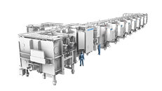
The MAX OLED solution is more than equipment: it begins with a proprietary pixel architecture built using a patented manufacturing recipe that results in best-in-class OLED pixels and displays. The manufacturing system combines a number of critical manufacturing modules in a single, high-vacuum system that protects the delicate OLED materials from the environment and reduces yield-killing particles. The MAX OLED system integrates display glass handling, multiple OLED deposition steps, and OLED encapsulation. Many of the core technologies used by the MAX OLED solution have already been proven by Applied in making large-area LCD screens at panel sizes up to Gen 10.5.
The MAX OLED solution reduces the energy consumption of OLED display fabs, requires significantly less OLED materials, and eliminates the need for mask cleaning chemicals, thereby reducing the environmental impact of display manufacturing.
A Growing OLED Display Opportunity
Applied is already the world's largest provider of display manufacturing equipment, with a broad portfolio of products spanning CVD and PVD deposition, CVD thin-film encapsulation, and eBeam testing and inspection. The MAX OLED solution is expected to more than double Applied's served addressable market opportunity in OLED display manufacturing.
Gen 6 glass panel surface area = 2.78 square meters; Gen 8 surface area = 5.5 square meters; Gen 10 surface area = 9.9 square meters
PVD = physical vapor deposition; CVD = chemical vapor deposition
View at TechPowerUp Main Site | Source
OLED is the display technology of choice for the world's leading smartphone manufacturers because it offers superior display quality, light and flexible form factors, and durability. However, until today, it has proven challenging to scale OLED display manufacturing to the larger glass panels used to make displays for tablets, PCs and TVs.

Applied's MAX OLED solution makes it easier to scale OLED manufacturing from Gen 6 glass substrates to Gen 8 substrates, which are approximately two times larger, and beyond. In addition, the MAX OLED solution deposits OLED materials in a new way that increases pixel brightness and resolution, reduces display energy consumption, and lengthens display lifetime.
The MAX OLED solution has strong customer interest, with repeat orders from multiple leading display manufacturers. Additionally, Applied will supply a MAX OLED solution to Samsung Display, a leading global manufacturer of OLED and QD-OLED panels. Samsung Display will be bringing in an alpha system to assess this new technology.
"The consumer electronics industry has been waiting for a breakthrough that can bring OLED technology to the hundreds of millions of tablets, PCs and TVs sold each year," said Dr. Brian Shieh, Group Vice President and General Manager of Applied's Display and Flexible Technology business. "We are proud to be partnering with Samsung Display to help bring this revolutionary technology to the global marketplace."
Making OLED Displays Brighter, Longer-Lasting and More Energy-Efficient
OLED displays are difficult to manufacture because the materials used to emit red, green and blue are fragile and ruined by any exposure to air or moisture. Applied's MAX OLED solution is a breakthrough technology that deposits and encapsulates each pixel individually using a specially designed maskless process. Applied's approach is precise, fast and superior at maintaining the purity of delicate OLED materials.
Applied's proprietary solution uses selective deposition to enable excellent pixel placement accuracy, more than doubling the amount of OLED material per area as compared to previous technologies. The technology can increase OLED display brightness by as much as 3X and increase resolution by as much as 2.5X, to approximately 2,000 pixels per square inch. The solution can also reduce display power consumption by more than 30 percent and increase display lifetime by up to 5X.
"Applied Materials has developed a true breakthrough in OLED manufacturing technology that will enable better OLED displays at more attractive prices," said Ross Young, Co-founder and CEO of Display Supply Chain Consultants (DSCC). "This technology has the potential to accelerate OLED adoption in a range of markets, from tablets and PCs to automobiles and micro-displays for AR/VR, creating a catalyst for the entire display industry."
New OLED Pixel Architecture, Process Recipe and Integrated Materials Solution
The MAX OLED solution is more than equipment: it begins with a proprietary pixel architecture built using a patented manufacturing recipe that results in best-in-class OLED pixels and displays. The manufacturing system combines a number of critical manufacturing modules in a single, high-vacuum system that protects the delicate OLED materials from the environment and reduces yield-killing particles. The MAX OLED system integrates display glass handling, multiple OLED deposition steps, and OLED encapsulation. Many of the core technologies used by the MAX OLED solution have already been proven by Applied in making large-area LCD screens at panel sizes up to Gen 10.5.
The MAX OLED solution reduces the energy consumption of OLED display fabs, requires significantly less OLED materials, and eliminates the need for mask cleaning chemicals, thereby reducing the environmental impact of display manufacturing.
A Growing OLED Display Opportunity
Applied is already the world's largest provider of display manufacturing equipment, with a broad portfolio of products spanning CVD and PVD deposition, CVD thin-film encapsulation, and eBeam testing and inspection. The MAX OLED solution is expected to more than double Applied's served addressable market opportunity in OLED display manufacturing.
Gen 6 glass panel surface area = 2.78 square meters; Gen 8 surface area = 5.5 square meters; Gen 10 surface area = 9.9 square meters
PVD = physical vapor deposition; CVD = chemical vapor deposition
View at TechPowerUp Main Site | Source

