- Joined
- Aug 19, 2017
- Messages
- 2,952 (1.06/day)
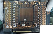
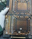
NVIDIA's GeForce RTX 5090 graphics card printed circuit board has allegedly been shown in the flesh, showing the memory layout and some interesting engineering choices. The custom PCB variant (non-Founders Edition) houses more than 40 capacitors, which is perhaps not standard on the FE reference board, and 16 GDDR7 memory modules. The leaked PCB, which extends beyond standard dimensions and traditional display connector configurations, is reportedly based on NVIDIA's PG145 reference design. The memory modules are distributed systematically: five on the left, two below, five on the right, and four above the GPU die. The interface is PCIe 5.0 x16.
As NVIDIA has reportedly designated 32 GB GDDR7 memory capacity for these cards, this roughly translates into 16 x 2 GB GDDR7 memory modules. At the heart of the card lies what sources claim to be the GB202 GPU, measuring 24×31 mm within a 63×56 mm package. Power delivery uses a 16-pin 12V-6x2 power connector, as expected. The entire PCB features only a single power connector, so the 16-pin 12V-2x6, but with an updated PCIe 6.0 CEM specification, is the logical choice.


View at TechPowerUp Main Site | Source
As NVIDIA has reportedly designated 32 GB GDDR7 memory capacity for these cards, this roughly translates into 16 x 2 GB GDDR7 memory modules. At the heart of the card lies what sources claim to be the GB202 GPU, measuring 24×31 mm within a 63×56 mm package. Power delivery uses a 16-pin 12V-6x2 power connector, as expected. The entire PCB features only a single power connector, so the 16-pin 12V-2x6, but with an updated PCIe 6.0 CEM specification, is the logical choice.


View at TechPowerUp Main Site | Source


 .
.


