T0@st
News Editor
- Joined
- Mar 7, 2023
- Messages
- 2,780 (3.69/day)
- Location
- South East, UK
| System Name | The TPU Typewriter |
|---|---|
| Processor | AMD Ryzen 5 5600 (non-X) |
| Motherboard | GIGABYTE B550M DS3H Micro ATX |
| Cooling | DeepCool AS500 |
| Memory | Kingston Fury Renegade RGB 32 GB (2 x 16 GB) DDR4-3600 CL16 |
| Video Card(s) | PowerColor Radeon RX 7800 XT 16 GB Hellhound OC |
| Storage | Samsung 980 Pro 1 TB M.2-2280 PCIe 4.0 X4 NVME SSD |
| Display(s) | Lenovo Legion Y27q-20 27" QHD IPS monitor |
| Case | GameMax Spark M-ATX (re-badged Jonsbo D30) |
| Audio Device(s) | FiiO K7 Desktop DAC/Amp + Philips Fidelio X3 headphones, or ARTTI T10 Planar IEMs |
| Power Supply | ADATA XPG CORE Reactor 650 W 80+ Gold ATX |
| Mouse | Roccat Kone Pro Air |
| Keyboard | Cooler Master MasterKeys Pro L |
| Software | Windows 10 64-bit Home Edition |
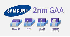
Reports from last November suggested that Samsung Electronics had semi-abandoned its second-generation 3 nm Gate-All-Around (GAA) process, due to missed production goals. Disappointing production yields—as low as 20%—have been floated by industry insiders, they believed (at the time) that the South Korean's foundry teams had simply moved onto developing a next-gen 2 nm manufacturing process. A freshly published news article, courtesy of Business Korea, provides further evidence of a shift to 2 nanometer processes—Samsung's S3 plant in Hwaseong is reportedly in the process of being upgraded (from 3 nm GAA). Insiders believe that new equipment will be installed across the existing production line, requiring a small-scale investment of funds.
The Pyeongtaek 2 (P2) plant is supposedly being prepared for a 1.4 nm test line—targeting a manufacturing capacity of 2000 to 3000 wafers per month. Inside track information suggests that trials will begin within the year. Business Korea's report suggests that Samsung has halved its foundry facility investment budget for 2025—around 5 trillion won, instead of last year's 10 trillion won. The article puts a spotlight on alleged "sluggish customer orders"—the primary factor behind Samsung's decision to slash its chip-making budget by 50%. Competition is fierce at this point in time—TSMC leads the way with its cutting-edge technologies. Taiwan's premier foundry has attracted many high-profile clients away from rival manufacturers. In contrast, industry watchdogs believe that Samsung's struggles have caused "big tech" customers to seek alternate channels.

View at TechPowerUp Main Site | Source
The Pyeongtaek 2 (P2) plant is supposedly being prepared for a 1.4 nm test line—targeting a manufacturing capacity of 2000 to 3000 wafers per month. Inside track information suggests that trials will begin within the year. Business Korea's report suggests that Samsung has halved its foundry facility investment budget for 2025—around 5 trillion won, instead of last year's 10 trillion won. The article puts a spotlight on alleged "sluggish customer orders"—the primary factor behind Samsung's decision to slash its chip-making budget by 50%. Competition is fierce at this point in time—TSMC leads the way with its cutting-edge technologies. Taiwan's premier foundry has attracted many high-profile clients away from rival manufacturers. In contrast, industry watchdogs believe that Samsung's struggles have caused "big tech" customers to seek alternate channels.


View at TechPowerUp Main Site | Source


