- Joined
- Oct 9, 2007
- Messages
- 47,895 (7.38/day)
- Location
- Dublin, Ireland
| System Name | RBMK-1000 |
|---|---|
| Processor | AMD Ryzen 7 5700G |
| Motherboard | Gigabyte B550 AORUS Elite V2 |
| Cooling | DeepCool Gammax L240 V2 |
| Memory | 2x 16GB DDR4-3200 |
| Video Card(s) | Galax RTX 4070 Ti EX |
| Storage | Samsung 990 1TB |
| Display(s) | BenQ 1440p 60 Hz 27-inch |
| Case | Corsair Carbide 100R |
| Audio Device(s) | ASUS SupremeFX S1220A |
| Power Supply | Cooler Master MWE Gold 650W |
| Mouse | ASUS ROG Strix Impact |
| Keyboard | Gamdias Hermes E2 |
| Software | Windows 11 Pro |
With wide-spread news about AMD integrating a graphics controller on a CPU, the AMD Fusion, the concept of "Small is Big" is being redefined. Fusion may look like a step in the right direction but is merely prelude to another computing methodology, the SoC (system on a chip). Fusion could be confined to consumer desktop/notebook central processing with graphics thrown in, but a concrete step taken by Intel into this which is more of targeted to the enterprise, embedded systems and consumer electronics is the EP80579 integrated processor. HotHardware spoke with Gadi Singer, Vice President of Intel's Mobility Group, and Doug Davis, Vice President of Intel's Digital Enterprise Group. Intel's brand new product line targeted at security, storage, communications, and industrial applications, basically embedded computing were discussed. The EP80579 integrated processor was central to this conversation. The need for this product came about by Intel as a preparation of the company for the impending onslaught of smart, Internet-connected devices and appliances predicted to arrive over the next few years.


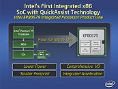
In simple terms, this is a processor, northbridge (with graphics controller), and southbridge rolled into one. The EP80579 consists of a block layout of system components as in the schematic in the first slide. It consists of a Pentium M processing core, a memory controller hub (MCH), I/O hub (ICH) and a PCI-Express switch. Components of the SoC communicate using a front side bus (FSB). Also developed is a high performance bus to connect the security, TDM, and data path acceleration engines to the I/O Complex, these features are what make up the Intel QuickAssist Technology, which isn't standard to every Intel EP80579 SoC.


The one main goal of this concept is to miniaturize the system, to minimize the energy footprint of the system, making it suitable for incorporation into a host of products in the consumer electronics and appliances industry. In some cases, Intel claims they will lead to platforms that have a 45% smaller board footprint and 34% lower power dissipation. Another implication is that Intel plans to miniaturize the IA x86 architecture to a level at which it competes directly with other architectures, and at a higher level, a propagation of the IA x86 architecture.
Intel also disclosed that they have more than 15 projects planned internally for the further development of this concept, some of which incorporate the Atom core, which would be consumer electronics ready, codenamed 'Canmore' that would be introduced later this year, and a next generation product slated for 2009 codenamed 'Sodaville' which shares its launch time-frame with "Moorestown", the company's next-gen platform for Mobile Internet Devices (MID).


View at TechPowerUp Main Site


In simple terms, this is a processor, northbridge (with graphics controller), and southbridge rolled into one. The EP80579 consists of a block layout of system components as in the schematic in the first slide. It consists of a Pentium M processing core, a memory controller hub (MCH), I/O hub (ICH) and a PCI-Express switch. Components of the SoC communicate using a front side bus (FSB). Also developed is a high performance bus to connect the security, TDM, and data path acceleration engines to the I/O Complex, these features are what make up the Intel QuickAssist Technology, which isn't standard to every Intel EP80579 SoC.


The one main goal of this concept is to miniaturize the system, to minimize the energy footprint of the system, making it suitable for incorporation into a host of products in the consumer electronics and appliances industry. In some cases, Intel claims they will lead to platforms that have a 45% smaller board footprint and 34% lower power dissipation. Another implication is that Intel plans to miniaturize the IA x86 architecture to a level at which it competes directly with other architectures, and at a higher level, a propagation of the IA x86 architecture.
Intel also disclosed that they have more than 15 projects planned internally for the further development of this concept, some of which incorporate the Atom core, which would be consumer electronics ready, codenamed 'Canmore' that would be introduced later this year, and a next generation product slated for 2009 codenamed 'Sodaville' which shares its launch time-frame with "Moorestown", the company's next-gen platform for Mobile Internet Devices (MID).


View at TechPowerUp Main Site
