- Joined
- Oct 9, 2007
- Messages
- 47,235 (7.55/day)
- Location
- Hyderabad, India
| System Name | RBMK-1000 |
|---|---|
| Processor | AMD Ryzen 7 5700G |
| Motherboard | ASUS ROG Strix B450-E Gaming |
| Cooling | DeepCool Gammax L240 V2 |
| Memory | 2x 8GB G.Skill Sniper X |
| Video Card(s) | Palit GeForce RTX 2080 SUPER GameRock |
| Storage | Western Digital Black NVMe 512GB |
| Display(s) | BenQ 1440p 60 Hz 27-inch |
| Case | Corsair Carbide 100R |
| Audio Device(s) | ASUS SupremeFX S1220A |
| Power Supply | Cooler Master MWE Gold 650W |
| Mouse | ASUS ROG Strix Impact |
| Keyboard | Gamdias Hermes E2 |
| Software | Windows 11 Pro |
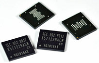
Samsung Electronics Co., Ltd., the world leader in advanced semiconductor technology solutions, today announced the industry's first multi-chip package (MCP) with PRAM - for use in mobile handsets beginning later this quarter.
The 512 megabit Samsung PRAM in the MCP is backward compatible with 40 nanometer-class* NOR flash memory in both its hardware and software functionality, allowing mobile handset designers the convenience of having multi-chip packaging fully compatible with past stand-alone PRAM chip technology. PRAM is expected to be widely embraced by next year as the successor to NOR flash in consumer electronics designs, to become a major memory technology.

"Memories for portable consumer devices today are at a major turning point as mobile applications increasingly require more diverse memory technologies," said Dong-soo Jun, executive vice president, Memory Sales and Marketing, Samsung Electronics. "The launch of our PRAM in an advanced MCP solution for the replacement of 40nm-class and finer geometry NOR meets this need head-on. Our PRAM MCP will not only enable handset designers to utilize conventional platforms, but expedite the introduction of LPDDR2 DRAM and next-generation PRAM technology as the leading-edge basis for high-performance solutions," he added.
PRAM, which stores data via the phase change characteristics of its base material, an alloy of germanium, antimony and titanium, provides three-times faster data storage performance per word than NOR chips. This new PRAM-packaged memory combines the nonvolatile nature of flash memory with the high-speed capability of DRAM. Its simple cell structure makes designing MCP chips for handsets a faster and easier process, with the imminent use of 30nm-class and finer process node technology to overcome long-time design difficulties inherent in NOR flash technology.
As a replacement for NOR, PRAM can more easily accommodate the growing demand for high-speed, high-density nonvolatile memory in mobile phones and other mobile applications such as MP3 players, personal multimedia players and navigational devices.
Samsung is continuing its research and development into PRAM and other advanced memory chips to enable faster 'write' capabilities, a key feature in taking photo images, providing multimedia messaging and recording video clips to reduce the standby time in data storage. This high-speed write capability will be important in a diverse span of digital storage and consumer devices, such as solid state drives (SSDs) and HDTVs.
View at TechPowerUp Main Site
The 512 megabit Samsung PRAM in the MCP is backward compatible with 40 nanometer-class* NOR flash memory in both its hardware and software functionality, allowing mobile handset designers the convenience of having multi-chip packaging fully compatible with past stand-alone PRAM chip technology. PRAM is expected to be widely embraced by next year as the successor to NOR flash in consumer electronics designs, to become a major memory technology.

"Memories for portable consumer devices today are at a major turning point as mobile applications increasingly require more diverse memory technologies," said Dong-soo Jun, executive vice president, Memory Sales and Marketing, Samsung Electronics. "The launch of our PRAM in an advanced MCP solution for the replacement of 40nm-class and finer geometry NOR meets this need head-on. Our PRAM MCP will not only enable handset designers to utilize conventional platforms, but expedite the introduction of LPDDR2 DRAM and next-generation PRAM technology as the leading-edge basis for high-performance solutions," he added.
PRAM, which stores data via the phase change characteristics of its base material, an alloy of germanium, antimony and titanium, provides three-times faster data storage performance per word than NOR chips. This new PRAM-packaged memory combines the nonvolatile nature of flash memory with the high-speed capability of DRAM. Its simple cell structure makes designing MCP chips for handsets a faster and easier process, with the imminent use of 30nm-class and finer process node technology to overcome long-time design difficulties inherent in NOR flash technology.
As a replacement for NOR, PRAM can more easily accommodate the growing demand for high-speed, high-density nonvolatile memory in mobile phones and other mobile applications such as MP3 players, personal multimedia players and navigational devices.
Samsung is continuing its research and development into PRAM and other advanced memory chips to enable faster 'write' capabilities, a key feature in taking photo images, providing multimedia messaging and recording video clips to reduce the standby time in data storage. This high-speed write capability will be important in a diverse span of digital storage and consumer devices, such as solid state drives (SSDs) and HDTVs.
View at TechPowerUp Main Site


