Raevenlord
News Editor
- Joined
- Aug 12, 2016
- Messages
- 3,755 (1.24/day)
- Location
- Portugal
| System Name | The Ryzening |
|---|---|
| Processor | AMD Ryzen 9 5900X |
| Motherboard | MSI X570 MAG TOMAHAWK |
| Cooling | Lian Li Galahad 360mm AIO |
| Memory | 32 GB G.Skill Trident Z F4-3733 (4x 8 GB) |
| Video Card(s) | Gigabyte RTX 3070 Ti |
| Storage | Boot: Transcend MTE220S 2TB, Kintson A2000 1TB, Seagate Firewolf Pro 14 TB |
| Display(s) | Acer Nitro VG270UP (1440p 144 Hz IPS) |
| Case | Lian Li O11DX Dynamic White |
| Audio Device(s) | iFi Audio Zen DAC |
| Power Supply | Seasonic Focus+ 750 W |
| Mouse | Cooler Master Masterkeys Lite L |
| Keyboard | Cooler Master Masterkeys Lite L |
| Software | Windows 10 x64 |
Intel is undoubtedly at the forefront of silicon processing technology these days, and has been for a long time. Being a fully integrated company from the bottom up, through the design and actual production of its silicon semiconductors, really does have a way of either paying of tremendously (as has been the case with Intel), or not at all (as was the case with AMD). That fabrication processes' nm ratings don't mean much in thhe industry right now has been the case for a while now; different companies use different calculations towards achieving a 22 nm or 14 nm claim, with some components in the same nm process having almost double the size of the same components in a competitor's equivalent. Intel has always been one of the more adamant defenders of an industry-wide categorization, both to avoid confusion and - naturally - put into perspective their process leadership.


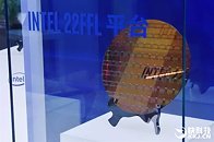
That process leadership should extend towards the 10 nm realms, where the company is looking to improve transistor density by around 2.7x. The product where Intel is going to start production on the process is a smart one for the company: FPGAs. As we all know, new manufacturing processes typically feature lower yields than more mature ones; as such, manufacture of monolithic, high die-size processing solutions isn't the best option (even though it's what happens often0. The smarter thing to do would be to have initial production being set to a product that doesn't care too much about wafer defects that could invalidate a full product. FPGAs are the most likely candidate due to their extremely redundant nature, in that a defect wouldn't bring about catastrophic issues with the affected chips; Intel can simply disable individual gate arrays with defects and cycle them through appropriate binning.


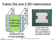
That is the main reason why Intel is putting its "Falcon Mesa" FPGA architecture to the test with the 10nm process. This allows the ocmpany to further tune the 10 nm production process with a relatively low-risk product, that's less sensitive to yield issues and defects, while earing up towards ramp-up of their more critical products - mainly CPUs. The "Falcon Mesa" FPGA design will also leverage Intel's EMIB packaging solution, where packaging of the chips is done with additional silicon substrates that allow for the connection and quicker data transfer between separate silicon blocks. This obviates the need for a full silicon interposer as AMD uses with its Vega graphics cards - a more effective, but much more expensive way of doing this. This means that Intel doesn't need to manufacture all of a chips' components on the same relatively low-yield, higher-risk 10 nm process - they can use other, "legacy" process nodes (14 nm, or even 22 nm) for parts that aren't critical in terms of power consumption or that don't require cutting-edge manufacturing.


View at TechPowerUp Main Site


That process leadership should extend towards the 10 nm realms, where the company is looking to improve transistor density by around 2.7x. The product where Intel is going to start production on the process is a smart one for the company: FPGAs. As we all know, new manufacturing processes typically feature lower yields than more mature ones; as such, manufacture of monolithic, high die-size processing solutions isn't the best option (even though it's what happens often0. The smarter thing to do would be to have initial production being set to a product that doesn't care too much about wafer defects that could invalidate a full product. FPGAs are the most likely candidate due to their extremely redundant nature, in that a defect wouldn't bring about catastrophic issues with the affected chips; Intel can simply disable individual gate arrays with defects and cycle them through appropriate binning.


That is the main reason why Intel is putting its "Falcon Mesa" FPGA architecture to the test with the 10nm process. This allows the ocmpany to further tune the 10 nm production process with a relatively low-risk product, that's less sensitive to yield issues and defects, while earing up towards ramp-up of their more critical products - mainly CPUs. The "Falcon Mesa" FPGA design will also leverage Intel's EMIB packaging solution, where packaging of the chips is done with additional silicon substrates that allow for the connection and quicker data transfer between separate silicon blocks. This obviates the need for a full silicon interposer as AMD uses with its Vega graphics cards - a more effective, but much more expensive way of doing this. This means that Intel doesn't need to manufacture all of a chips' components on the same relatively low-yield, higher-risk 10 nm process - they can use other, "legacy" process nodes (14 nm, or even 22 nm) for parts that aren't critical in terms of power consumption or that don't require cutting-edge manufacturing.


View at TechPowerUp Main Site

