• Welcome to TechPowerUp Forums, Guest! Please check out our forum guidelines for info related to our community.
  • The forums have been upgraded with support for dark mode. By default it will follow the setting on your system/browser. You may override it by scrolling to the end of the page and clicking the gears icon.

Xbox Head Posts "Project Scarlett" (Xbox Series X) SoC Picture, Has that 7nm Tinge

btarunr

Editor & Senior Moderator
Staff member
Joined
Oct 9, 2007
Messages
47,850 (7.39/day)
Location
Dublin, Ireland
System Name RBMK-1000
Processor AMD Ryzen 7 5700G
Motherboard Gigabyte B550 AORUS Elite V2
Cooling DeepCool Gammax L240 V2
Memory 2x 16GB DDR4-3200
Video Card(s) Galax RTX 4070 Ti EX
Storage Samsung 990 1TB
Display(s) BenQ 1440p 60 Hz 27-inch
Case Corsair Carbide 100R
Audio Device(s) ASUS SupremeFX S1220A
Power Supply Cooler Master MWE Gold 650W
Mouse ASUS ROG Strix Impact
Keyboard Gamdias Hermes E2
Software Windows 11 Pro
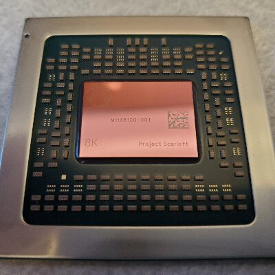
Phil Spencer, head of the Xbox division at Microsoft, posted a picture of the semi-custom SoC at the heart of the company's upcoming "Project Scarlett" Xbox Series X game console as his Twitter avatar. The picture reveals a chip that looks visibly similar to that of "Project Scorpio" (Xbox One X). The picture was also taken from an angle that reveals the pinkish/auburn tinge of 7 nm AMD chips made at TSMC. You'll find the same tinge on chips such as "Navi 10" when viewed from an angle. The die unabashedly bears the "Project Scarlett" and "8K" markings.

Next-generation game consoles are marketing 4K 60 Hz and 8K gaming capability. They likely use a combination of dynamic resolution-scale and variable rate shading to achieve this. The "Project Scarlett" SoC is a semi-custom chip co-designed by Microsoft and AMD, and uses CPU cores based on the company's "Zen 2" microarchitecture, combined with a powerful GPU based on RDNA2, which features hardware-accelerated ray-tracing and variable-rate shading. Hardware enthusiasts on Twitter are abuzz with estimating the die-size of the SoC, with calculations pinning it around the 350 mm² mark ±10 mm², or roughly similar to that of "Project Scorpio," but one must factor in the switch to 7 nm from 16 nm significantly increasing transistor-density.


View at TechPowerUp Main Site
 
"Our calculations put the Xbox Scarlett APU at roughly 401mm², which is an increase of almost 42mm² over the Xbox Scorpio chip at 359mm²."

Xbox-Scarlett-Die-Size-Comparison-1480x789.jpg


Scorpio had 2560 SPs with 2 CUs disabled and while the Xbox Scarlett APU is clearly bigger, it is not possible to speculate based just on the die size because of the different process node involved (7nm vs 16nm) but we can safely say that you are looking at at least 50% more power in the same die space. Since the Scorpio APU can output roughly 6 TFLOPs of power, we can guesstimate a range of at least 9 TFLOPs for the Scarlett APU ( up to 12 TFLOPS is within the realm of possibility).
 
Last edited:
"Our calculations put the Xbox Scarlett APU at roughly 401mm², which is an increase of almost 42mm² over the Xbox Scorpio chip at 359mm²."

Xbox-Scarlett-Die-Size-Comparison-1480x789.jpg


Scorpio had 2560 SPs with 2 CUs disabled and while the Xbox Scarlett APU is clearly bigger, it is not possible to speculate based just on the die size because of the different process node involved (7nm vs 16nm) but we can safely say that you are looking at at least 50% more power in the same die space. Since the Scorpio APU can output roughly 6 TFLOPs of power, we can guesstimate a range of at least 9 TFLOPs for the Scarlett APU ( up to 12 TFLOPS is within the realm of possibility).
They're not counting Zen CPU are they, unlike AMD with their APU's in the past?
 
RDNA is looking to be a really nice design. HW accelerated RTRT; Variable Rate Shading. As long as the driver support is good it will bring some healthy competition to the table.
 
What's the 8K about on the bottom left of the HS?.

Tbf i was shocked n awed by the geeky chip shot, so much so i forgot to read, niiice.
 
350 mm² mark ±10 mm²

I.e no 3584 shaders as it was supposedly leaked. Not for now at least, maybe there will be a faster version in the future.
 
Considering the 5700XT is 251mm2 and a Zen 2 8 core chiplet is around 70-80mm2 This console is going to be pretty interesting from a performance standpoint. I can't wait to see what the Forza Horizon 4 team pumps out on this as it will probably also greatly improve the PC version.
 
Looks solid enough, and with game devs taking advantage of such tech can only help PC arch like Turing finally unleash their shackles.
 
Can anybody pull its Rapid Packed Math spec? Vega was GCN5 for instance, GCN5+ reserved for RDNA2 isn't found on Timothy Lottes white paper.
 
That means if we're talking about an APU, it would put Scarlett at ~16 billion transistors on a 7nm process.
 
Can anybody pull its Rapid Packed Math spec? Vega was GCN5 for instance, GCN5+ reserved for RDNA2 isn't found on Timothy Lottes white paper.
RDNA based Navi gpus do support Rapid Packed math. Though Xbox use custom GPU, so it could support RPM or not.
 
With consoles supporting cross-play and keyboard and mouse... This may be the console that takes me away from PC gaming.
 
RDNA based Navi gpus do support Rapid Packed math. Though Xbox use custom GPU, so it could support RPM or not.
RPM is instrumental to Radeon legacy in the consoles. GCN5 can compute a result per 1.5 operations, so this changes how much compute TFLOPS is available fundamentally.
 
What's the 8K about on the bottom left of the HS?.
8K is video decoding. Bluray (if it has a player) and streaming.

It could render 2D games at 8K but vast majority of them will be 4K.
 
Back
Top