TheLostSwede
News Editor
- Joined
- Nov 11, 2004
- Messages
- 18,319 (2.46/day)
- Location
- Sweden
| System Name | Overlord Mk MLI |
|---|---|
| Processor | AMD Ryzen 7 7800X3D |
| Motherboard | Gigabyte X670E Aorus Master |
| Cooling | Noctua NH-D15 SE with offsets |
| Memory | 32GB Team T-Create Expert DDR5 6000 MHz @ CL30-34-34-68 |
| Video Card(s) | Gainward GeForce RTX 4080 Phantom GS |
| Storage | 1TB Solidigm P44 Pro, 2 TB Corsair MP600 Pro, 2TB Kingston KC3000 |
| Display(s) | Acer XV272K LVbmiipruzx 4K@160Hz |
| Case | Fractal Design Torrent Compact |
| Audio Device(s) | Corsair Virtuoso SE |
| Power Supply | be quiet! Pure Power 12 M 850 W |
| Mouse | Logitech G502 Lightspeed |
| Keyboard | Corsair K70 Max |
| Software | Windows 10 Pro |
| Benchmark Scores | https://valid.x86.fr/yfsd9w |
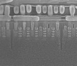
Semiconductor industry research firm TechInsights said it has found that Samsung's 3 nm GAA (gate-all-around) process has been incorporated into the crypto miner ASIC (Whatsminer M56S++) from a Chinese manufacturer, MicroBT. In a Disruptive Technology Event Brief exclusively provided to DIGITIMES Asia, TechInsights points out that the significance of this development lies in the commercial utilization of GAA technology, which facilitates the scaling of transistors to 2 nm and beyond. "This development is crucial because it has the potential to enhance performance, improve energy efficiency, keep up with Moore's Law, and enable advanced applications," said TechInsights, identifying the MicroBT ASIC chip the first commercialized product using GAA technology in the industry.
But this would also reveal that Samsung is the foundry for MicroBT, using the 3 nm GAA process. DIGITIMES Research semiconductor analyst Eric Chen pointed out that Samsung indeed has started producing chips using the 3 nm GAA process, but the capacity is still small. "Getting revenues from shipment can be defined as 'commercialization', but ASIC is a relatively simple kind of chip to produce, in terms of architecture."
DIGITIMES analyst John Wang highlighted the fact that the yield of Samsung's 3 nm GAA process is still low, so it will try to get as many customers as possible to help train its processes and improve the yield. It is understandable why they would do business with a Chinese customer.
However, just like the SMIC 7 nm process previously found by TechInsights in a MinerVa Bitcoin mining chip, analysts said the fact that the 3 nm process is proved manufacturable does not necessarily mean it has achieved a satisfactory yield that can generate commercial value for the foundry at the current level.
Samsung claims its first-generation 3 nm process could reduce power consumption by 45%, increase performance by 23%, and reduce chip area by 16% compared to 5 nm technology, promising even more advances for future generations.
View at TechPowerUp Main Site | Source
But this would also reveal that Samsung is the foundry for MicroBT, using the 3 nm GAA process. DIGITIMES Research semiconductor analyst Eric Chen pointed out that Samsung indeed has started producing chips using the 3 nm GAA process, but the capacity is still small. "Getting revenues from shipment can be defined as 'commercialization', but ASIC is a relatively simple kind of chip to produce, in terms of architecture."


DIGITIMES analyst John Wang highlighted the fact that the yield of Samsung's 3 nm GAA process is still low, so it will try to get as many customers as possible to help train its processes and improve the yield. It is understandable why they would do business with a Chinese customer.
However, just like the SMIC 7 nm process previously found by TechInsights in a MinerVa Bitcoin mining chip, analysts said the fact that the 3 nm process is proved manufacturable does not necessarily mean it has achieved a satisfactory yield that can generate commercial value for the foundry at the current level.
Samsung claims its first-generation 3 nm process could reduce power consumption by 45%, increase performance by 23%, and reduce chip area by 16% compared to 5 nm technology, promising even more advances for future generations.
View at TechPowerUp Main Site | Source