TheLostSwede
News Editor
- Joined
- Nov 11, 2004
- Messages
- 18,319 (2.46/day)
- Location
- Sweden
| System Name | Overlord Mk MLI |
|---|---|
| Processor | AMD Ryzen 7 7800X3D |
| Motherboard | Gigabyte X670E Aorus Master |
| Cooling | Noctua NH-D15 SE with offsets |
| Memory | 32GB Team T-Create Expert DDR5 6000 MHz @ CL30-34-34-68 |
| Video Card(s) | Gainward GeForce RTX 4080 Phantom GS |
| Storage | 1TB Solidigm P44 Pro, 2 TB Corsair MP600 Pro, 2TB Kingston KC3000 |
| Display(s) | Acer XV272K LVbmiipruzx 4K@160Hz |
| Case | Fractal Design Torrent Compact |
| Audio Device(s) | Corsair Virtuoso SE |
| Power Supply | be quiet! Pure Power 12 M 850 W |
| Mouse | Logitech G502 Lightspeed |
| Keyboard | Corsair K70 Max |
| Software | Windows 10 Pro |
| Benchmark Scores | https://valid.x86.fr/yfsd9w |
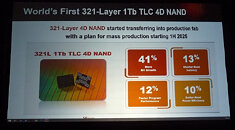
Courtesy of an SK Hynix keynote speech at the Flash Memory Summit, we now have a few more details about its upcoming 321-layer NAND Flash. PC Watch Japan who attended the industry event shared some pictures from the keynote which adds some crucial details that were missing from last week's press release. SK Hynix's officially shared performance figures tell us that we should expect up to 12 percent faster program performance, which should be the write performance and up to 13 percent improved read latency. Both of these performance metrics will obviously depend on the SSD controller the NAND is paired with, the related firmware on said controller and so forth.
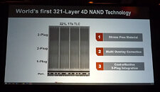
PC Watch Japan also quotes a program throughput of 194 MB/s, which is 26 MB/s improvement over SK Hynix 176-layer NAND and currently the highest known program throughput of any announced NAND Flash. That said, Kioxia is expecting to hit 205 MB/s with its next generation of 300 layer NAND. SK Hynix also claims 10 percent better read power efficiency, which is really neither here nor there when it comes to modern SSDs, unless we're talking server level SSDs with a dozen of these NAND chips or more. Rather than going with two stacks of 150 plus layers each, SK Hynix went with three times 107 layer stacks, which should be compared to their current 238 layer product which has two stacks of 119 layers. This made the new NAND package easier to produce and should in the long term result in higher yields. Each NAND package is expected to deliver a memory density of 20 Gbit per square millimetre or more, which is almost twice that of its 176-layer NAND.


View at TechPowerUp Main Site | Source
PC Watch Japan also quotes a program throughput of 194 MB/s, which is 26 MB/s improvement over SK Hynix 176-layer NAND and currently the highest known program throughput of any announced NAND Flash. That said, Kioxia is expecting to hit 205 MB/s with its next generation of 300 layer NAND. SK Hynix also claims 10 percent better read power efficiency, which is really neither here nor there when it comes to modern SSDs, unless we're talking server level SSDs with a dozen of these NAND chips or more. Rather than going with two stacks of 150 plus layers each, SK Hynix went with three times 107 layer stacks, which should be compared to their current 238 layer product which has two stacks of 119 layers. This made the new NAND package easier to produce and should in the long term result in higher yields. Each NAND package is expected to deliver a memory density of 20 Gbit per square millimetre or more, which is almost twice that of its 176-layer NAND.


View at TechPowerUp Main Site | Source


