T0@st
News Editor
- Joined
- Mar 7, 2023
- Messages
- 2,177 (3.19/day)
- Location
- South East, UK
Lee Kang-Wook, Vice President of Research and Development at SK Hynix, has discussed the increased importance of advanced chip packaging with Bloomberg News. In an interview with the media company's business section, Lee referred to a tradition of prioritizing the design and fabrication of chips: "the first 50 years of the semiconductor industry has been about the front-end." He believes that the latter half of production processes will take precedence in the future: "...but the next 50 years is going to be all about the back-end." He outlined a "more than $1 billion" investment into South Korean facilities—his department is hoping to "improve the final steps" of chip manufacturing.
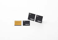
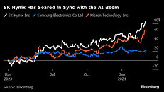
SK Hynix's Head of Packaging Development pioneered a novel method of packaging the third generation of high bandwidth technology (HBM2E)—that innovation secured NVIDIA as a high-profile and long term customer. Demand for Team Green's AI GPUs has boosted the significance of HBM technologies—Micron and Samsung are attempting to play catch up with new designs. South Korea's leading memory supplier is hoping to stay ahead in the next-gen HBM contest—supposedly 12-layer fifth generation samples have been submitted to NVIDIA for approval. SK Hynix's Vice President recently revealed that HBM production volumes for 2024 have sold out—currently company leadership is considering the next steps for market dominance in 2025. The majority of the firm's newly announced $1 billion budget will be spent on the advancement of MR-MUF and TSV technologies, according to their R&D chief.

View at TechPowerUp Main Site | Source
SK Hynix's Head of Packaging Development pioneered a novel method of packaging the third generation of high bandwidth technology (HBM2E)—that innovation secured NVIDIA as a high-profile and long term customer. Demand for Team Green's AI GPUs has boosted the significance of HBM technologies—Micron and Samsung are attempting to play catch up with new designs. South Korea's leading memory supplier is hoping to stay ahead in the next-gen HBM contest—supposedly 12-layer fifth generation samples have been submitted to NVIDIA for approval. SK Hynix's Vice President recently revealed that HBM production volumes for 2024 have sold out—currently company leadership is considering the next steps for market dominance in 2025. The majority of the firm's newly announced $1 billion budget will be spent on the advancement of MR-MUF and TSV technologies, according to their R&D chief.


View at TechPowerUp Main Site | Source


