- Joined
- Aug 19, 2017
- Messages
- 3,201 (1.11/day)
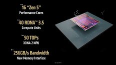
Thanks to the informative breakdown by Chips and Cheese, we are learning that AMD's latest Ryzen AI processors for laptops, codenamed "Strix Halo," utilize a parallel "sea of wires" interconnect system between their chiplets, replacing the SERDES (serializer/deserializer) approach found in desktop Ryzen models. The processor's physical implementation consists of two Core Complex Dies (CCDs), each manufactured on TSMC's N4 (4 nm) process and containing up to eight Zen 5 cores with full 512-bit floating point units. Notably, the I/O die (IOD) is also produced using the N4 process, marking an advancement from the N6 (6 nm) process used in standard Ryzen IODs on desktops. The key change lies in the inter-chiplet communication system. While the Ryzen 9000 series (Granite Ridge) employs SERDES to convert parallel data to serial for transmission between chiplets, Strix Halo implements direct parallel data transmission through multiple physical connections.
This design achieves 32 bytes per clock cycle throughput and eliminates the latency overhead associated with serialization/deserialization processes. The parallel interconnect architecture also removes the need for connection retraining during power state transitions, a limitation present in SERDES implementations. However, this design choice necessitates additional substrate complexity due to increased connection density and requires more pins for external connections, suggesting possible modifications to the CCD design compared to desktop variants. AMD's implementation required more complex substrate manufacturing processes to accommodate the dense parallel connections between chiplets. The decision to prioritize this more challenging design approach was driven by requirements for lower latency and power consumption in data-intensive workloads, where consistent high-bandwidth communication between chiplets is crucial.

View at TechPowerUp Main Site | Source
This design achieves 32 bytes per clock cycle throughput and eliminates the latency overhead associated with serialization/deserialization processes. The parallel interconnect architecture also removes the need for connection retraining during power state transitions, a limitation present in SERDES implementations. However, this design choice necessitates additional substrate complexity due to increased connection density and requires more pins for external connections, suggesting possible modifications to the CCD design compared to desktop variants. AMD's implementation required more complex substrate manufacturing processes to accommodate the dense parallel connections between chiplets. The decision to prioritize this more challenging design approach was driven by requirements for lower latency and power consumption in data-intensive workloads, where consistent high-bandwidth communication between chiplets is crucial.

View at TechPowerUp Main Site | Source


