• Welcome to TechPowerUp Forums, Guest! Please check out our forum guidelines for info related to our community.

AMD Ryzen AI Max+ "Strix Halo" Die Exposed and Annotated

AleksandarK

News Editor
Staff member
Joined
Aug 19, 2017
Messages
2,804 (1.02/day)
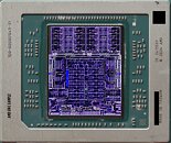
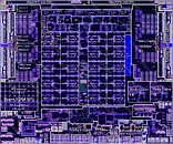
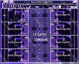
AMD's "Strix Halo" APU, marketed as Ryzen AI Max+, has just been exposed in die-shot analysis. Confirming the processor's triple-die architecture, the package showcases a total silicon footprint of 441.72 mm² that integrates advanced CPU, GPU, and AI acceleration capabilities within a single package. The processor's architecture centers on two 67.07 mm² CPU CCDs, each housing eight Zen 5 cores with a dedicated 8 MB L2 cache. A substantial 307.58 mm² I/O complements these die that houses an RDNA 3.5-based integrated GPU featuring 40 CUs and AMD's XDNA 2 NPU. The memory subsystem demonstrates a 256-bit LPDDR5X interface capable of delivering 256 GB/s bandwidth, supported by 32 MB of strategically placed Last Level Cache to optimize data throughput.

The die shots reveal notable optimizations for mobile deployment, including shortened die-to-die interfaces that reduce the interconnect distance by 2 mm compared to desktop implementations. Some through-silicon via structures are present, which suggest potential compatibility with AMD's 3D V-Cache technology, though the company has not officially confirmed plans for such implementations. The I/O die integrates comprehensive connectivity options, including PCIe 4.0 x16 lanes and USB4 support, while also housing dedicated media engines with full AV1 codec support. Initial deployments of the Strix Halo APU will commence with the ASUS ROG Flow Z13 launch on February 25, marking the beginning of what AMD anticipates will be broad adoption across premium mobile computing platforms.


View at TechPowerUp Main Site | Source
 
Joined
Dec 12, 2016
Messages
2,274 (0.76/day)
It looks like a single CCD has an MTr/mm^2 of 128.2. That's the same as the 5090. 4 nm confirmed!
 
Joined
Aug 12, 2022
Messages
265 (0.29/day)
AMD told Chips and Cheese that these are literally the same CCDs that go into Ryzen 9000, which is indeed using TSMC N4P.
 
Joined
Aug 22, 2016
Messages
174 (0.06/day)
It looks like a single CCD has an MTr/mm^2 of 128.2. That's the same as the 5090. 4 nm confirmed!
The process is called 4n, and the N stands for Nvidia. That's just the original 5nm with some Nvidia mods, just like Ada was. Its Nvidia 5nm confirmed.

AMD told Chips and Cheese that these are literally the same CCDs that go into Ryzen 9000, which is indeed using TSMC N4P.
In the same interview, they say this chip uses an organic substrate to connect the CCDs with lower latency and power than the desktop parts.
 
Joined
Feb 25, 2012
Messages
65 (0.01/day)
The IO looks like a regular GPU. Even USB controllers look fine. Modern graphics cards are equipped with USB-C ports.
 
Joined
Jan 3, 2021
Messages
3,858 (2.55/day)
Location
Slovenia
Processor i5-6600K
Motherboard Asus Z170A
Cooling some cheap Cooler Master Hyper 103 or similar
Memory 16GB DDR4-2400
Video Card(s) IGP
Storage Samsung 850 EVO 250GB
Display(s) 2x Oldell 24" 1920x1200
Case Bitfenix Nova white windowless non-mesh
Audio Device(s) E-mu 1212m PCI
Power Supply Seasonic G-360
Mouse Logitech Marble trackball, never had a mouse
Keyboard Key Tronic KT2000, no Win key because 1994
Software Oldwin
In the same interview, they say this chip uses an organic substrate to connect the CCDs with lower latency and power than the desktop parts.
Desktop parts use organic substrate, and the huge number of wires is the reason IOD can't be placed closer to CCDs. This APU seems to include something more advanced that enables the chips to sit next to each other. It could be Local Si Interconnect (LSI), which is approximately the TSMC's version of EMIB.
 
Joined
Oct 6, 2021
Messages
1,723 (1.40/day)
System Name Raspberry Pi 7 Quantum @ Overclocked.
AMD absolutely nailed the first generation with minimal setbacks. I never expected an MCM APU with 16 fucking cores to deliver such solid battery life while going toe-to-toe with Apple; despite using an inferior process node and lacking mac OS-level optimization. I can’t help but wonder how powerful the "Halo next-gen" will be, especially given the overwhelmingly positive reception.
 
Joined
Aug 25, 2021
Messages
1,275 (1.00/day)
n the same interview, they say this chip uses an organic substrate to connect the CCDs with lower latency and power than the desktop parts.
Yes, a new version of Fanout Infinity Link with organic interposer. They used something similar on Navi 31 to connect MCDs to GCD. Infinity Link brings a lot more density and bandwidth than Infinity Fabric.

Screenshot 2025-02-19 at 00-22-57 AMD ZEN 6 — Next-gen Chiplets & Packaging - YouTube.png


It looks like they are trialing this interconnect on Strix Halo and they will implement it across Zen6 chiplets and IOD as a new high-bandwidth, low latency and high-efficiency interconnect standard. Quite exciting, indeed.


The IO looks like a regular GPU. Even USB controllers look fine. Modern graphics cards are equipped with USB-C ports.
No. Regular GPU die has less diverse logic and functions than IOD.
Some modern GPUs have USB-C port as an interface for DP video signal, and not for carrying USB or PCIe data.

On Strix Halo IOD, USB3 and USB4 PHY are additional pieces of logic, as well as NPU, which are not present on GPU die.
 
Joined
Jan 3, 2021
Messages
3,858 (2.55/day)
Location
Slovenia
Processor i5-6600K
Motherboard Asus Z170A
Cooling some cheap Cooler Master Hyper 103 or similar
Memory 16GB DDR4-2400
Video Card(s) IGP
Storage Samsung 850 EVO 250GB
Display(s) 2x Oldell 24" 1920x1200
Case Bitfenix Nova white windowless non-mesh
Audio Device(s) E-mu 1212m PCI
Power Supply Seasonic G-360
Mouse Logitech Marble trackball, never had a mouse
Keyboard Key Tronic KT2000, no Win key because 1994
Software Oldwin
Yes, a new version of Fanout Infinity Link with organic interposer. They used something similar on Navi 31 to connect MCDs to GCD. Infinity Link brings a lot more density and bandwidth than Infinity Fabric.
Is this the same as RDL (Re-Distribution Layer)? In my (limited) understanding, RDL is a thin and dense multilayer PCB, which is bonded as a whole, or maybe built layer by layer, on top of the organic substrate, under the chiplets. AMD didn't want to disclose if they used it in Navi 31 or MI300, at least not initially.

AMD absolutely nailed the first generation with minimal setbacks.
It is 1st gen but a lot of experience building MCMs has been funneled into this product. AMD could call it "Instinct AI 101", it would seem right.

Imagine they got rid of the NPU and give up 8 more CU's.
Just an idea: CPU thread scheduling is so hard that no one can get it right these days, and "AI" has the potential to help here. If AMD and MS wanted of course.
 
Last edited:
Joined
Aug 25, 2021
Messages
1,275 (1.00/day)
Imagine they got rid of the NPU and give up 8 more CU's.
Not now. NPU is needed for AI workloads, power management, other productivity tasks, etc. Its size takes space of 12 CUs. They need NPU on a chip like this for further development, as the next gen of NPU should go over 100 TOPS. As the logic shrinks in the next gen, they will be able to add more CUs and IO on a die.

It took them four iterations to come to this maximum size design for the package used. It's better to have such product in the market than wait another year or so for yet another lab chip iteration to be perfected. It's more practical the way it is.

Is this thread same as RDL (Re-Distribution Layer)? In my (limited) understanding, RDL is a thin and dense multilayer PCB, which is bonded as a whole, or maybe built layer by layer, on top of the organic substrate, under the chiplets. AMD didn't want to disclose if they used it in Navi 31 or MI300, at least not initially.
Final MI300 is CoWoS-S, though they did have CoWoS-R as test chip. Navi 31 uses InFO-R/oS packaging with 4 RDL layers.

For Strix Halo, we don't know, until we know. It's either InFO-R or InFO-L, or another interation.
 
Joined
Feb 25, 2012
Messages
65 (0.01/day)
No. Regular GPU die has less diverse logic and functions than IOD.
Some modern GPUs have USB-C port as an interface for DP video signal, and not for carrying USB or PCIe data.

On Strix Halo IOD, USB3 and USB4 PHY are additional pieces of logic, as well as NPU, which are not present on GPU die.
nv tensor cores are not NPU?
 
Joined
Jan 3, 2021
Messages
3,858 (2.55/day)
Location
Slovenia
Processor i5-6600K
Motherboard Asus Z170A
Cooling some cheap Cooler Master Hyper 103 or similar
Memory 16GB DDR4-2400
Video Card(s) IGP
Storage Samsung 850 EVO 250GB
Display(s) 2x Oldell 24" 1920x1200
Case Bitfenix Nova white windowless non-mesh
Audio Device(s) E-mu 1212m PCI
Power Supply Seasonic G-360
Mouse Logitech Marble trackball, never had a mouse
Keyboard Key Tronic KT2000, no Win key because 1994
Software Oldwin
Joined
Aug 25, 2021
Messages
1,275 (1.00/day)
nv tensor cores are not NPU?
Tensor cores are found in SMs. Each SM integrates specialized hardware, including tensor cores, RT cores, texture units, etc., whereas NPU is a separate, dedicated logic on mobility APUs for neural processing. Two different designs.
 
Joined
Dec 17, 2024
Messages
91 (1.38/day)
Not now. NPU is needed for AI workloads, power management, other productivity tasks, etc. Its size takes space of 12 CUs. They need NPU on a chip like this for further development, as the next gen of NPU should go over 100 TOPS. As the logic shrinks in the next gen, they will be able to add more CUs and IO on a die.
Is the NPU actually, technically needed zo ? AFAIK power management has never needed a dedicated NPU, nor did AI tasks.

It seems to me that it "needs" to be there only due to Microsoft's commercial tantrum.
 
Joined
May 7, 2020
Messages
159 (0.09/day)
Desktop parts use organic substrate, and the huge number of wires is the reason IOD can't be placed closer to CCDs. This APU seems to include something more advanced that enables the chips to sit next to each other. It could be Local Si Interconnect (LSI), which is approximately the TSMC's version of EMIB.
the first picture shows the IFOP on CCDs and IOD perfectly aligned, something that would be impossible with the N6 IOD on desktop. This alone could what allows thedies to be put next to each other
 
Joined
Aug 25, 2021
Messages
1,275 (1.00/day)
Is the NPU actually, technically needed zo ? AFAIK power management has never needed a dedicated NPU, nor did AI tasks.
It seems to me that it "needs" to be there only due to Microsoft's commercial tantrum.
It is needed if equivalent AI acceleration, similar in function to tensor cores, cannot be found integrated within GPU cores.
 
Joined
Nov 14, 2021
Messages
148 (0.12/day)
Is the NPU actually, technically needed zo ? AFAIK power management has never needed a dedicated NPU, nor did AI tasks.

It seems to me that it "needs" to be there only due to Microsoft's commercial tantrum.
Jim Kelly has an interview somewhere since he has been at Tenstorrent. I remember the convo being something in regards to him talking to a PSU engineer, and even they could benefit from a micro ML processor that costs a couple bucks. NPUs will eventually be in all kinds of devices.

Do you technically need NPU capabilities? Sure don't. Just like you technically don't need RT capabilities to run RT stuff. You can do it all on a GPU with RT cores or even a CPU. It'll just be slower and use more energy. NPU can do something the CPU could do, but it'll do it much faster and use a lot less power. It's kinda why general processors can have multiple fixed function processors/engines on the same package.
 
Joined
May 10, 2023
Messages
607 (0.93/day)
Location
Brazil
Processor 5950x
Motherboard B550 ProArt
Cooling Fuma 2
Memory 4x32GB 3200MHz Corsair LPX
Video Card(s) 2x RTX 3090
Display(s) LG 42" C2 4k OLED
Power Supply XPG Core Reactor 850W
Software I use Arch btw
It is needed if equivalent AI acceleration, similar in function to tensor cores, cannot be found integrated within GPU cores.
Tensor cores are more general than NPUs tho, as in data types, and they require more power than a bare NPU as well.
AMD's software stack is still lacking when it comes to using their GPUs for ML acceleration, I guess that's why they are shoving an NPU in this product.
 
Top