malware
New Member
- Joined
- Nov 7, 2004
- Messages
- 5,422 (0.74/day)
- Location
- Bulgaria
| Processor | Intel Core 2 Quad Q6600 G0 VID: 1.2125 |
|---|---|
| Motherboard | GIGABYTE GA-P35-DS3P rev.2.0 |
| Cooling | Thermalright Ultra-120 eXtreme + Noctua NF-S12 Fan |
| Memory | 4x1 GB PQI DDR2 PC2-6400 |
| Video Card(s) | Colorful iGame Radeon HD 4890 1 GB GDDR5 |
| Storage | 2x 500 GB Seagate Barracuda 7200.11 32 MB RAID0 |
| Display(s) | BenQ G2400W 24-inch WideScreen LCD |
| Case | Cooler Master COSMOS RC-1000 (sold), Cooler Master HAF-932 (delivered) |
| Audio Device(s) | Creative X-Fi XtremeMusic + Logitech Z-5500 Digital THX |
| Power Supply | Chieftec CFT-1000G-DF 1kW |
| Software | Laptop: Lenovo 3000 N200 C2DT2310/3GB/120GB/GF7300/15.4"/Razer |
At the 2007 Optical Fiber Conference, IBM scientists will reveal a prototype optical transceiver chipset capable of reaching speeds at least eight times faster than optical components available today. The breakthrough could transform how data is accessed, shared and used across the Web for corporate and consumer networks. The transceiver is fast enough to reduce the download time for a typical high definition feature-length film to a single second compared to 30 minutes or more.

The ability to move information at blazing speeds of 160 Gigabits - or 160 billion bits of information in a single second - provides a glimpse of a new era of high-speed connectivity that will transform communications, computing and entertainment. Optical networking offers the potential to dramatically improve data transfer rates by speeding the flow of data using light pulses, instead of sending electrons over wires.
"The explosion in the amount of data being transferred, when downloading movies, TV shows, music or photos, is creating demand for greater bandwidth and higher speeds in connectivity," said Dr. T.C. Chen, vice president, Science & Technology, IBM Research. "Greater use of optical communications is needed to address this issue. We believe our optical transceiver technology may provide the answer."
As the amount of data transmitted over networks continues to grow, researchers have been looking for ways to make the use of optical signals more practical. The ability to use these signals could offer previously unheard of amounts of bandwidth and enhanced signal fidelity compared to current electrical data links. By shrinking and integrating the components into one package, and building them with standard low-cost, high-volume chip manufacturing techniques, IBM is making optical connectivity viable for widespread use.
For example, the technology could be integrated onto printed circuit boards to allow the components within an electronic system - such as a PC or set top box - to communicate much faster, dramatically enhancing the performance of the system itself.
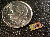
To achieve this new level of integration in the chipset, IBM researchers built an optical transceiver with driver and receiver integrated circuits in current CMOS technology, the same standard, high-volume, low-cost technology used for most chips today. They then coupled it with other necessary optical components made in more exotic materials, such as indium phosphide (InP) and gallium arsenide (GaAs), into one, integrated package only 3.25 by 5.25 millimeters in size.
This compact design provides both a high number of communications channels as well as very high speeds per channel, resulting in an amount of information transmitted per unit area of card space taken up by the chipset (the ultimate measure of viability for practical use) that is the highest ever. This transceiver chipset is designed to enable low cost optics by attaching to an optical printed circuit board employing densely spaced polymer waveguide channels using mass assembly processes.
The report on this work, "160-Gb/s, 16-Channel Full-Duplex, Single-Chip CMOS Optical Transceiver," by C.L. Schow, F.E. Doany, O. Liboiron-Ladouceur, C. Baks, D.M. Kuchta, L. Schares, R. John, and J.A. Kash of IBM's T. J. Watson Research Center, Yorktown Heights, N.Y. will be presented on March 29 at the 2007 Optical Fiber Conference in Anaheim. This work was partially funded by Defense Advanced Research Project Agency through the Chip to Chip Optical Interconnect (C2OI) program.
View at TechPowerUp Main Site


 .
.

