• Welcome to TechPowerUp Forums, Guest! Please check out our forum guidelines for info related to our community.

Editorial On The Coming Chiplet Revolution and AMD's MCM Promise

Raevenlord

News Editor
Joined
Aug 12, 2016
Messages
3,755 (1.25/day)
Location
Portugal
System Name The Ryzening
Processor AMD Ryzen 9 5900X
Motherboard MSI X570 MAG TOMAHAWK
Cooling Lian Li Galahad 360mm AIO
Memory 32 GB G.Skill Trident Z F4-3733 (4x 8 GB)
Video Card(s) Gigabyte RTX 3070 Ti
Storage Boot: Transcend MTE220S 2TB, Kintson A2000 1TB, Seagate Firewolf Pro 14 TB
Display(s) Acer Nitro VG270UP (1440p 144 Hz IPS)
Case Lian Li O11DX Dynamic White
Audio Device(s) iFi Audio Zen DAC
Power Supply Seasonic Focus+ 750 W
Mouse Cooler Master Masterkeys Lite L
Keyboard Cooler Master Masterkeys Lite L
Software Windows 10 x64
With Moore's Law being pronounced as within its death throes, historic monolithic die designs are becoming increasingly expensive to manufacture. It's no secret that both AMD and NVIDIA have been exploring an MCM (Multi-Chip-Module) approach towards diverting from monolithic die designs over to a much more manageable, "chiplet" design. Essentially, AMD has achieved this in different ways with its Zen line of CPUs (two CPU modules of four cores each linked via the company's Infinity Fabric interconnect), and their own R9 and Vega graphics cards, which take another approach in packaging memory and the graphics processing die in the same silicon base - an interposer.
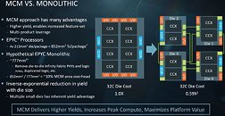
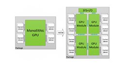
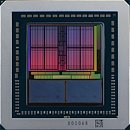


This "chiplet" approach is easy to understand - smaller, leaner chips can be produced with higher yields than large, monolithic ones, which are more prone to silicon defects. This increased yield (and increased number of chips per wafer, in the end) allows AMD to reduce manufacturing costs and increase production efficiency by using a single mask for a quad-core module, for instance. Afterwards, it's "simply" a matter of scaling the number of modules to the desired amount and performance paradigm - from eight-core Ryzen CPUs to 32-core Threadripper II CPUs. However, as the number of modules in a given chip increase, so does complexity of signal processing and routing - two modules communicating with each other is relatively easy to achieve, but six or eight modules? Not so much, as a small hiccup in information transmission can deadlock the entire processor (speaking of either CPU or GPU designs here now). The challenge becomes increasingly greater when joining different types of chips - from memory to processing dies and I/O controllers - in a single silicon slice. This is where interposers appear - and where AMD is taking strides towards achieving an active interposer design.
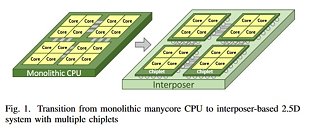
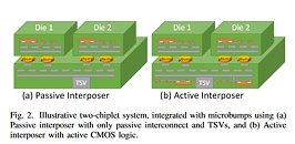

Passive interposers - such as the one found in the AMD Vega graphics cards - are simply a "dumb", silicon-enabler of data transmission - information is sent exactly as it was engineered to with the TSV (Through Silicon Vias) design. However, this approach is insufficient in the dream, open approach to chip integration - where manufacturers can create their designs, purchase other chips from other companies, and mix and match according to their end-product requirement. A "dumb", passive interposer won't suffice here - data routing problems would have to be manually solved with each different implementation, which is prohibitive from the cost perspective, and a big no-no for the approach. The solution, as AMD puts it on their "Cost-Effective Design of Scalable High-Performance Systems Using Active and Passive Interposers" paper, can be found, at least partially, with an active interposer - an interposer that features network logic (NoC - Network on Chip) that can adapt to the different slices of silicon grafted onto it. And this isn't just theoretics - active interposer designs have been manufactured, showing "improved signaling and efficiency over passive interposer [design]).

A big problem for this active interposer approach, however, is cost - again, the end of many promising technologies. AMD, however, is actively working on building enough redundancy in the active interposer design that yields aren't much of a concern - achieving the sweetspot between development cost and yield ratio. Nothing is worse than paying for a big-area, active interposer die with all of its network circuitry and have it have such defects that it can't be used.

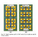

For now, AMD says these active interposers ought to be reserved for high-performance designs - not surprising, given the added R&D cost over passive interposer or sans-interposer design. The dream to mix and match and reuse different IPs at will via a "simple" substrate, however, is very much alive. AMD researchers proved that for 32-core processors - with possibilities of scaling with estimated monolithic die complexity versus the chiplet approach - could be achieved with much better yield and lower manufacturing cost in the chiplet + passive /active interposer design versus a monolithic 16 nm die.
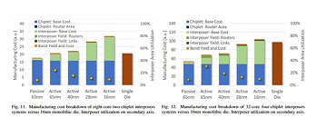


The process used to fabricate the interposer is very important here - so as to increase yield ratios, 65 nm through 28 nm active or passive solutions provide reduced development and manufacturing costs. Active interposers, while more expensive than their passive counterparts, add the aforementioned networking capabilities that allow for zero deadlock possibility, routing signals as needed between different components of the design.

View at TechPowerUp Main Site
 
Joined
Oct 18, 2013
Messages
6,167 (1.52/day)
Location
Over here, right where you least expect me to be !
System Name The Little One
Processor i5-11320H @4.4GHZ
Motherboard AZW SEI
Cooling Fan w/heat pipes + side & rear vents
Memory 64GB Crucial DDR4-3200 (2x 32GB)
Video Card(s) Iris XE
Storage WD Black SN850X 4TB m.2, Seagate 2TB SSD + SN850 4TB x2 in an external enclosure
Display(s) 2x Samsung 43" & 2x 32"
Case Practically identical to a mac mini, just purrtier in slate blue, & with 3x usb ports on the front !
Audio Device(s) Yamaha ATS-1060 Bluetooth Soundbar & Subwoofer
Power Supply 65w brick
Mouse Logitech MX Master 2
Keyboard Logitech G613 mechanical wireless
Software Windows 10 pro 64 bit, with all the unnecessary background shitzu turned OFF !
Benchmark Scores PDQ
IIRC, some other company (fruity named) wanted to do this many many years ago to get around the ever-increasing mhz war chants, but their manufacturing partners had no clue how to implement the desired technical leap, so the idea died, or at least got covered in dust, until now anyways :)
 
Joined
Feb 18, 2005
Messages
5,815 (0.81/day)
Location
Ikenai borderline!
System Name Firelance.
Processor Threadripper 3960X
Motherboard ROG Strix TRX40-E Gaming
Cooling IceGem 360 + 6x Arctic Cooling P12
Memory 8x 16GB Patriot Viper DDR4-3200 CL16
Video Card(s) MSI GeForce RTX 4060 Ti Ventus 2X OC
Storage 2TB WD SN850X (boot), 4TB Crucial P3 (data)
Display(s) 3x AOC Q32E2N (32" 2560x1440 75Hz)
Case Enthoo Pro II Server Edition (Closed Panel) + 6 fans
Power Supply Fractal Design Ion+ 2 Platinum 760W
Mouse Logitech G602
Keyboard Razer Pro Type Ultra
Software Windows 10 Professional x64
Hmmm... I wonder if any of this is based on/derived from Intel's EMIB?
 
Joined
Mar 10, 2010
Messages
11,878 (2.22/day)
Location
Manchester uk
System Name RyzenGtEvo/ Asus strix scar II
Processor Amd R5 5900X/ Intel 8750H
Motherboard Crosshair hero8 impact/Asus
Cooling 360EK extreme rad+ 360$EK slim all push, cpu ek suprim Gpu full cover all EK
Memory Corsair Vengeance Rgb pro 3600cas14 16Gb in four sticks./16Gb/16GB
Video Card(s) Powercolour RX7900XT Reference/Rtx 2060
Storage Silicon power 2TB nvme/8Tb external/1Tb samsung Evo nvme 2Tb sata ssd/1Tb nvme
Display(s) Samsung UAE28"850R 4k freesync.dell shiter
Case Lianli 011 dynamic/strix scar2
Audio Device(s) Xfi creative 7.1 on board ,Yamaha dts av setup, corsair void pro headset
Power Supply corsair 1200Hxi/Asus stock
Mouse Roccat Kova/ Logitech G wireless
Keyboard Roccat Aimo 120
VR HMD Oculus rift
Software Win 10 Pro
Benchmark Scores 8726 vega 3dmark timespy/ laptop Timespy 6506
Hmmm... I wonder if any of this is based on/derived from Intel's EMIB?
No ,not at all it's mearly an evolutionary step , I've often pointed out quite correctly that every cpu has a circuit based interposer to interconnect the die and package to the socket type bar sorlder on type chips so why in gods name did anyone need to swap mother boards so often , anyway.
A silicon interposer is little different ,an active one makes this a 3d soc imho and a first.
Emib on the other hand is on chip fully, afaik it requires chips to conform with each other though a tsv version and 2.5d i suppose do make sense ,i might be wrong their i have not heard of anything bar chip to chip though, possibly better being so direct , maybe that's why Amd mentioned active to counter EMIB.
 
Joined
Apr 19, 2011
Messages
2,198 (0.44/day)
Location
So. Cal.
I would say while great in theory and showing promise, I thought the last I heard at least from AMD's perspective this long from any prime time solution to gaming and GPU. Their Infinity Fabric interconnect is not able to carry all the calls/responds that feed modern GPU's. The aim is gaming developers won't need do anything different in developing games. There's no added software or programing that needs to be don on their part as was the case with multi-GPU technologies like SLI/CF. They intend to make these MCM appear as nothing more than one bigger GPU and for that to happen the through-put and interconnect speed needs a much more speedy/robust cross-talk that as of yet Infinity Fabric has not (yet) provided.

I appreciate the update, but as I heard MCM for GPU is far from ready for primetime.
 
Joined
Sep 11, 2015
Messages
624 (0.19/day)
interconnect speed needs a much more speedy/robust cross-talk that as of yet Infinity Fabric has not (yet) provided.

I appreciate the update, but as I heard MCM for GPU is far from ready for primetime.
This article literally is saying "we know about this problem, and this is how we intend to change that". Did you read it?

It's one of the better articles on TPU I have read. We need more of this type of stuff, just this.
 
Joined
Nov 3, 2013
Messages
2,141 (0.53/day)
Location
Serbia
Processor Ryzen 5600
Motherboard X570 I Aorus Pro
Cooling Deepcool AG400
Memory HyperX Fury 2 x 8GB 3200 CL16
Video Card(s) RX 6700 10GB SWFT 309
Storage SX8200 Pro 512 / NV2 512
Display(s) 24G2U
Case NR200P
Power Supply Ion SFX 650
Mouse G703 (TTC Gold 60M)
Keyboard Keychron V1 (Akko Matcha Green) / Apex m500 (Gateron milky yellow)
Software W10
Well for Radeon it's either this or bust. At least by now they have ton of experience from Epyc and TR.
 
Joined
Sep 14, 2017
Messages
625 (0.24/day)
Whatever happens, its all pretty interesting and exciting. I wonder when full 3D designs will come into play.
 
Joined
Apr 12, 2013
Messages
7,507 (1.77/day)
Hmmm... I wonder if any of this is based on/derived from Intel's EMIB?
No, it's not. In fact EMIB doesn't solve Intel's problems wrt inter die high speed interconnect ala IF for AMD. That's why they hired keller, EMIB is a physical implementation but they still have to get something like IF for the bridge (EMIB) to not be a bottleneck in transferring vast amounts of data between the chips. IF is rated at a max of 512GBps & accordingly is the fastest interconnect out there, faster than Nvlink IIRC.
 
Joined
Oct 2, 2004
Messages
13,791 (1.88/day)
IIRC, some other company (fruity named) wanted to do this many many years ago to get around the ever-increasing mhz war chants, but their manufacturing partners had no clue how to implement the desired technical leap, so the idea died, or at least got covered in dust, until now anyways :)

Actually, the first one was 3dfx with its VSA100 chips. They could basically stack as many as they needed. Main 3dfx's problem was they were so ahead of time all that became their demise. If they were doing the stuff they were doing back then, things would probably work out great. Vega at 7nm is a refresh of last series, but with NAVI, it is predicted that they are using same approach they used for Ryzen. Stacking of smaller GPU cores to work as one. I frankly think that is indeed the future because making huge GPU's we have now has really crappy yields and that's just bad. But smaller cores have very high yields even with new nodes. It's just up to them to solve the intercore communication. But AMD has quite some experience even with that. From Ryzen and also from their older products where they used special "ring bus" designs to circulate necessary processing data between core logics. We'll see. But I hope it'll work out for them, because that might change the face of the gaming (and compute) industry quite dramatically.
 

btarunr

Editor & Senior Moderator
Staff member
Joined
Oct 9, 2007
Messages
47,200 (7.56/day)
Location
Hyderabad, India
System Name RBMK-1000
Processor AMD Ryzen 7 5700G
Motherboard ASUS ROG Strix B450-E Gaming
Cooling DeepCool Gammax L240 V2
Memory 2x 8GB G.Skill Sniper X
Video Card(s) Palit GeForce RTX 2080 SUPER GameRock
Storage Western Digital Black NVMe 512GB
Display(s) BenQ 1440p 60 Hz 27-inch
Case Corsair Carbide 100R
Audio Device(s) ASUS SupremeFX S1220A
Power Supply Cooler Master MWE Gold 650W
Mouse ASUS ROG Strix Impact
Keyboard Gamdias Hermes E2
Software Windows 11 Pro
Not sure if an interposer is needed for MCMs like EPYC. The InfinityFabric links between the dies don't have as many pins as GPU-to-HBM2 connections, and can make do with the fiberglass substrate.

An interposer only makes sense when you have a wast amount of wiring and not enough space to route them through a substrate.

MCM GPUs (made up of multiple GPU dies) won't work unless they're abstract to the host as one GPU (multi-GPU is dead), even then I can't begin to imagine the software side chaos of distributing workload between GPU dies while pretending that they make up one GPU (and not multi-GPU). Unless of course that MCM GPUs are being targeted at HPC/AI and not gamers.
 

FordGT90Concept

"I go fast!1!11!1!"
Joined
Oct 13, 2008
Messages
26,259 (4.47/day)
Location
IA, USA
System Name BY-2021
Processor AMD Ryzen 7 5800X (65w eco profile)
Motherboard MSI B550 Gaming Plus
Cooling Scythe Mugen (rev 5)
Memory 2 x Kingston HyperX DDR4-3200 32 GiB
Video Card(s) AMD Radeon RX 7900 XT
Storage Samsung 980 Pro, Seagate Exos X20 TB 7200 RPM
Display(s) Nixeus NX-EDG274K (3840x2160@144 DP) + Samsung SyncMaster 906BW (1440x900@60 HDMI-DVI)
Case Coolermaster HAF 932 w/ USB 3.0 5.25" bay + USB 3.2 (A+C) 3.5" bay
Audio Device(s) Realtek ALC1150, Micca OriGen+
Power Supply Enermax Platimax 850w
Mouse Nixeus REVEL-X
Keyboard Tesoro Excalibur
Software Windows 10 Home 64-bit
Benchmark Scores Faster than the tortoise; slower than the hare.
MCM GPUs (made up of multiple GPU dies) won't work unless they're abstract to the host as one GPU (multi-GPU is dead), even then I can't begin to imagine the software side chaos of distributing workload between GPU dies while pretending that they make up one GPU (and not multi-GPU). Unless of course that MCM GPUs are being targeted at HPC/AI and not gamers.
Exactly. It's going to require something far more complex than Infinity Fabric to do properly; hence, "active interposer" maybe?
 
Joined
Sep 15, 2007
Messages
3,946 (0.63/day)
Location
Police/Nanny State of America
Processor OCed 5800X3D
Motherboard Asucks C6H
Cooling Air
Memory 32GB
Video Card(s) OCed 6800XT
Storage NVMees
Display(s) 32" Dull curved 1440
Case Freebie glass idk
Audio Device(s) Sennheiser
Power Supply Don't even remember
Not sure if an interposer is needed for MCMs like EPYC. The InfinityFabric links between the dies don't have as many pins as GPU-to-HBM2 connections, and can make do with the fiberglass substrate.

An interposer only makes sense when you have a wast amount of wiring and not enough space to route them through a substrate.

MCM GPUs (made up of multiple GPU dies) won't work unless they're abstract to the host as one GPU (multi-GPU is dead), even then I can't begin to imagine the software side chaos of distributing workload between GPU dies while pretending that they make up one GPU (and not multi-GPU). Unless of course that MCM GPUs are being targeted at HPC/AI and not gamers.

I figured it would be fancy hardware scheduler/fetch with a big buffer on the front and whatever you call the stuff on the back end with large cache.
 
Last edited:
Joined
Feb 3, 2017
Messages
3,735 (1.32/day)
Processor Ryzen 7800X3D
Motherboard ROG STRIX B650E-F GAMING WIFI
Memory 2x16GB G.Skill Flare X5 DDR5-6000 CL36 (F5-6000J3636F16GX2-FX5)
Video Card(s) INNO3D GeForce RTX™ 4070 Ti SUPER TWIN X2
Storage 2TB Samsung 980 PRO, 4TB WD Black SN850X
Display(s) 42" LG C2 OLED, 27" ASUS PG279Q
Case Thermaltake Core P5
Power Supply Fractal Design Ion+ Platinum 760W
Mouse Corsair Dark Core RGB Pro SE
Keyboard Corsair K100 RGB
VR HMD HTC Vive Cosmos
MCM in TR/Epic works because the intended market/niche does not care about latency. Their implementation is technically not that much different from multi-socket server. That is the same reason thousands of GPUs in supercomputers are working just fine together. This is fine for CPUs as the work is generalized and granular enough. GPUs are massively parallel when it comes to computation units but there are control functions as well as hardware like TMU/ROP/etc that are performing rendering stages that cannot be easily distributed to different chips over reasonable link (not even wide IF or NVLink). At least not without some paradigm change in how work in GPUs is distrubuted. Current understanding and implementations of MCM GPU would fall into Crossfire/SLI category, the solutions that manufacturers are actively pulling out from.

EMIB resolves the problem with interposer size. Patents and implementation details will undoubtedly be an interesting fight we will see soon enough.

No, it's not. In fact EMIB doesn't solve Intel's problems wrt inter die high speed interconnect ala IF for AMD. That's why they hired keller, EMIB is a physical implementation but they still have to get something like IF for the bridge (EMIB) to not be a bottleneck in transferring vast amounts of data between the chips. IF is rated at a max of 512GBps & accordingly is the fastest interconnect out there, faster than Nvlink IIRC.
Infinity Fabric seems to have received more hype than it's worth. It is definitely awesome but it is not the only contemporary scalable interconnect out there.

AMD has Infinity Fabric:
AMD has stated the range to be 30 GB/s to 512 GB/s. Implementation details seem to be somewhat different depending on type of interconnect - in Zen's case inside (2x32 bits) or between chips (2x16 wires).
Actual implementation: In EPIC/TR/Ryzen each link inside chip has bandwidth 42 GB/s bi-directionally and between chips 38 GB/s bi-directionally. This is with the spec DDR4-2666 memory and 1333 MHz clock.

Nvidia has NVLink:
A channel (link) is 32 wires - 8-bit differential pairs (lanes) and bi-directional. 20 GT/s (or 25 for NVLink 2.0). Assuming NVLink 2.0, that is 25GB/s per link, 50GB/s bi-directional and can be scaled up with more links. NVLink's NVSwitch is 18-port and total bandwidth of 900 GB/s so NVLink by itself does seem to be scalable.
Actual implementation: Big Pascal has 4 NVLink 1.0 links - 80/160 GB/s, big Volta has 6 NVLink 2.0 links - 150/300 GB/s.

Intel has QPI (and soon UPI):
These are Intel's multi-CPU interconnects that have been evolving over time. Historically these tend to favor latency over bandwidth as that has been Intel's need. Currently, dual-socket Xeon systems actually have inter-CPU latencies that are nor far off from inter-chip IF in EPIC CPUs. As an interesting note, QPI is 20-lane link (40 data wires) logically divided into 4 quadrants, 5 lane each. These quadrants can be managed separately.
UPI is stated to have 10.4 GT/s and 2-3 UPI links per CPU which brings some management and power improvements but performance-wise is just the same interconnect as QPI running at max 5.2 GHz.
Actual Implementation: Initial implementation in Nehalem was running at 3.2 Ghz with resulting bandwidth of 25.6 GB/s. Haswell's implementation is running at 4.8 GHz and bandwidth 38.4 GB/s.
UPI will bring the bandwidth per link up to 41.6 GB/s.

This is just bandwidth. There are several other important considerations. Latency is one, power consumption is another, die space consumed becomes a problem at some amount of links as well.

I figured it would be fancy hardware scheduler/fetch with a big buffer on the front and whatever you call the stuff on the back end with large cache.
I think power is the primary consideration here. Powering the links on/through interposer conserves power when compared to links on/though PCB.
AMD has declared power efficiency as one of the wins of Infinity Fabric and it does consume a notable amount of power in TR/EPIC. Intel, in the same manner, is trying to reduce the power consumption going from QPI to UPI.

Exactly. It's going to require something far more complex than Infinity Fabric to do properly; hence, "active interposer" maybe?
The problem is not the link as much as managing traffic on a bunch of high-speed links. Interconnect itself will still be Infinity Fabric but the active part on the interposer will have to be a switch of some type.
But this is still a physical(ish) layer problem, software issues are on top of all this.

Actually, the first one was 3dfx with its VSA100 chips. They could basically stack as many as they needed. Main 3dfx's problem was they were so ahead of time all that became their demise. If they were doing the stuff they were doing back then, things would probably work out great. Vega at 7nm is a refresh of last series, but with NAVI, it is predicted that they are using same approach they used for Ryzen. Stacking of smaller GPU cores to work as one. I frankly think that is indeed the future because making huge GPU's we have now has really crappy yields and that's just bad. But smaller cores have very high yields even with new nodes. It's just up to them to solve the intercore communication. But AMD has quite some experience even with that. From Ryzen and also from their older products where they used special "ring bus" designs to circulate necessary processing data between core logics. We'll see. But I hope it'll work out for them, because that might change the face of the gaming (and compute) industry quite dramatically.
3dfx's approach to multiple chips was SLI (Scan-Line Interleave) that was employed on both multiple chips on Voodoo 4/5 cards as well as linking two separate Voodoo2 cards. Then, each chip simply rendered the next row of pixels. While the specific method has not been used for a long time, this type of work distribution is easily doable by both AMD and Nvidia today with Crossfire and SLI respectively. Unfortunately, GPU functionality as well as engines have become much more complex so these naive methods are too twitchy. Interconnect is not the problem here unless using a brute force method of using an extremely wide and low latency bus which is technically not viable.

AMD's GPU chief has now confirmed that Navi will not be an MCM approach and while they would like to (and most definitely do) explore this, it is not in the cards in foreseeable future.
 
Last edited:
Joined
Apr 19, 2011
Messages
2,198 (0.44/day)
Location
So. Cal.
This article literally is saying "we know about this problem, and this is how we intend to change that". Did you read it?

It's one of the better articles on TPU I have read. We need more of this type of stuff, just this.
I'm glad you found something interesting that ad's to the discussion... Not!

While I understand the article and it is good... while more technical for most, the only issue I kind of was looking to point out is this is still in a "theory stage" for GPU's. Even with interposer they have many huddles.

MCM GPUs (made up of multiple GPU dies) won't work unless they're abstract to the host as one GPU (multi-GPU is dead), even then I can't begin to imagine the software side chaos of distributing workload between GPU dies while pretending that they make up one GPU (and not multi-GPU). Unless of course that MCM GPUs are being targeted at HPC/AI and not gamers.
btarunr; as above basically offers the same issue I tried to add that wasn't explicit in the article. That was, the biggest evolution that needs to start working itself out and always the Achilles Heel of ground breaking technology have special individual competing technologies. Worst is as londiste post covers, everyone is in the throes of their competing implementations, with the hope all these implementations would come about so that each' companies implementation is imperceptible to greater use of outside software, drivers etc.
 
Last edited:
Joined
Sep 11, 2015
Messages
624 (0.19/day)
I'm glad you found something interesting that ad's to the discussion... Not!
And your comment was important how? Because you already know everything about how this is going to work?

An actually smart interposer is like having trafic lights instead of a single lane for all cars. It's potentially a very huge improvement to throughput, so I can't see how you can say "interconnect speed needs a much more speedy/robust cross-talk that as of yet Infinity Fabric has not (yet) provided" because you "heard" that "MCM for GPU is far from ready for primetime". This article literally and directly addresses the cross-talk problem and offers a new solution. Your comment makes no sense at all in light of this not being Infinity Fabric as it is right now, like it seems you're saying.
 
Joined
Apr 19, 2011
Messages
2,198 (0.44/day)
Location
So. Cal.
And your comment was important how? Because you already know everything about how this is going to work?
I was glad to see my response got you to present some thinking that's perspicuous and adds something germane to the topic.

Your comment makes no sense at all in light of this not being Infinity Fabric as it is right now, like it seems you're saying
I was working form recent information that was covering such topics less than 2 weeks ago. Were you aware of such articles?
https://www.pcgamesn.com/amd-navi-monolithic-gpu-design
https://www.tweaktown.com/news/62244/amd-ready-mcm-radeon-skip-navi-gpu-arch/index.html

I just saw this as "tantalizing" and more put-out there by AMD to deflect those earlier stories that MCM had hurdles, while help to displace what Raja Koduri had said about Vega a while back, that the Infinity Fabric interconnect would be the "perfect system" to splice a bunch of discrete GPUs together on a single ASIC design.

Then I don't find in the article talking about "traffic signal", best I read was improved signaling and efficiency over passive interposer. While at some point AMD can probably make this work as can others there are plenty of hurdles.
 
Last edited:

Garyhsp63

New Member
Joined
Jul 30, 2018
Messages
1 (0.00/day)
CoWoS - Passive Silicon Interposer
EMIB - Passive Silicon Bridge
Next should be Active Silicon Interposer and active Silicon Bridge
 
Top