- Joined
- Aug 19, 2017
- Messages
- 2,786 (1.02/day)
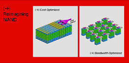
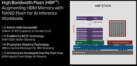
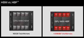
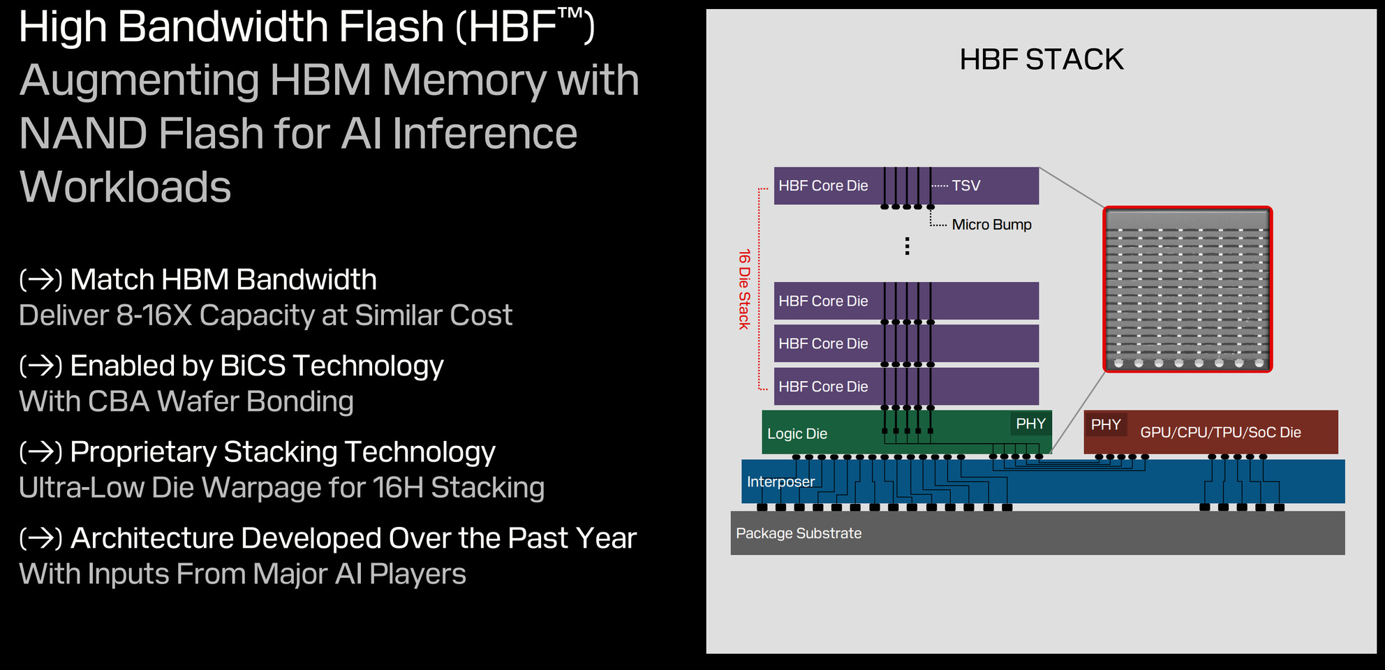
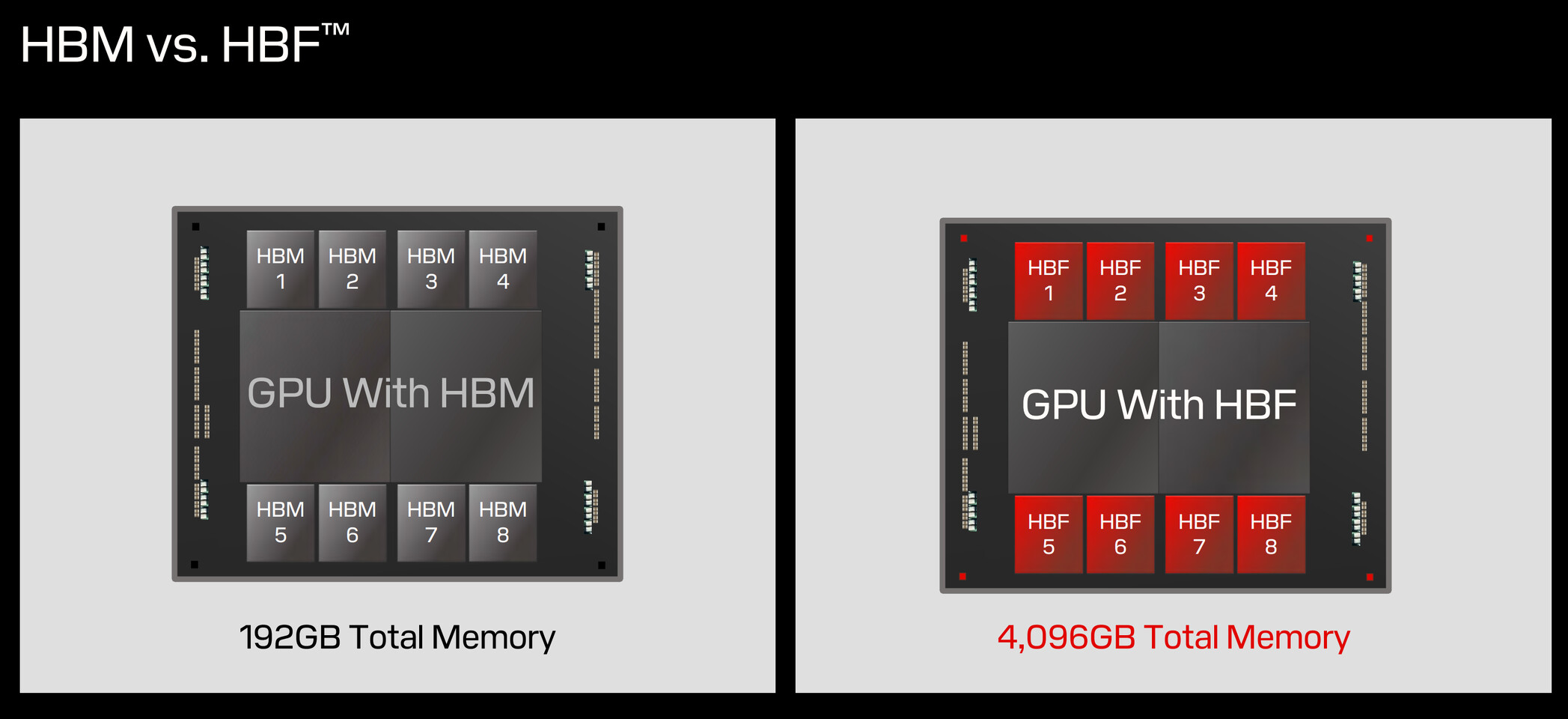
During its first post-Western Digital spinoff investor day, SanDisk showed something it has been working on to tackle the AI sector. High-bandwidth flash (HBF) is a new memory architecture that combines 3D NAND flash storage with bandwidth capabilities comparable to high-bandwidth memory (HBM). The HBF design stacks 16 3D NAND BiCS8 dies using through-silicon vias, with a logic layer enabling parallel access to memory sub-arrays. This configuration achieves 8 to 16 times greater capacity per stack than current HBM implementations. A system using eight HBF stacks can provide 4 TB of VRAM to store large AI models like GPT-4 directly on GPU hardware. The architecture breaks from conventional NAND design by implementing independently accessible memory sub-arrays, moving beyond traditional multi-plane approaches. While HBF surpasses HBM's capacity specifications, it maintains higher latency than DRAM, limiting its application to specific workloads.
SanDisk has not disclosed its solution for NAND's inherent write endurance limitations, though using pSLC NAND makes it possible to balance durability and cost. The bandwidth of HBF is also unknown, as the company hasn't put out details yet. SanDisk Memory Technology Chief Alper Ilkbahar confirmed the technology targets read-intensive AI inference tasks rather than latency-sensitive applications. The company is developing HBF as an open standard, incorporating mechanical and electrical interfaces similar to HBM to simplify integration. Some challenges remain, including NAND's block-level addressing limitations and writing endurance constraints. While these factors make HBF unsuitable for gaming applications, the technology's high capacity and throughput characteristics align with AI model storage and inference requirements. SanDisk has announced plans for three generations of HBF development, indicating a long-term commitment to the technology.
View at TechPowerUp Main Site | Source
SanDisk has not disclosed its solution for NAND's inherent write endurance limitations, though using pSLC NAND makes it possible to balance durability and cost. The bandwidth of HBF is also unknown, as the company hasn't put out details yet. SanDisk Memory Technology Chief Alper Ilkbahar confirmed the technology targets read-intensive AI inference tasks rather than latency-sensitive applications. The company is developing HBF as an open standard, incorporating mechanical and electrical interfaces similar to HBM to simplify integration. Some challenges remain, including NAND's block-level addressing limitations and writing endurance constraints. While these factors make HBF unsuitable for gaming applications, the technology's high capacity and throughput characteristics align with AI model storage and inference requirements. SanDisk has announced plans for three generations of HBF development, indicating a long-term commitment to the technology.

View at TechPowerUp Main Site | Source


