Report an Error

Intel Sandy Bridge GT1
SIC66SIC66
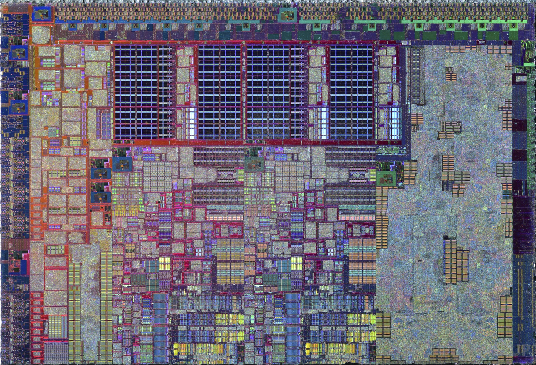
Die Shot
Intel's Sandy Bridge GT1 GPU uses the Generation 6.0 architecture and is made using a 32 nm production process at Intel. With a die size of 131 mm² and a transistor count of 504 million it is a small chip. Sandy Bridge GT1 supports DirectX 11.1 (Feature Level 10_1). Modern GPU compute technologies are not available. It features 48 shading units, 6 texture mapping units and 1 ROPs.
Graphics Processor
- Released
- Feb 1st, 2011
- GPU Name
- Sandy Bridge GT1
- Architecture
- Generation 6.0
- Foundry
- Intel
- Process Size
- 32 nm
- Transistors
- 504 million
- Density
- 3.8M / mm²
- Die Size
- 131 mm²
Graphics Features
- DirectX
- 11.1 (10_1)
- OpenGL
- 3.1
- OpenCL
- N/A
- Vulkan
- N/A
- Shader Model
- 4.1
Render Config
- Shading Units
- 48
- TMUs
- 6
- ROPs
- 1
- Execution Units
- 6
All Generation 6.0 GPUs
- Intel Sandy Bridge GT1
- Intel Sandy Bridge GT2
- Intel Sandy Bridge GT2+
Intel GPU Architecture History
- 2023 Xe-LPG
- 2022-2023 Generation 12.7
- 2021-2024 Generation 12.5
- 2021-2023 Generation 12.2
- 2020-2021 Generation 12.1
- 2019-2021 Generation 11.0
- 2016-2020 Generation 9.5
- 2015-2016 Generation 9.0
- 2014-2015 Generation 8.0
- 2013 Generation 7.5
- 2012-2013 Generation 7.0
- 2011 Generation 6.0
- 2010-2013 Knights
- 2010 Generation 5.75
- 2008-2010 PowerVR SGX545
- 2008 Generation 5.0
- 2008-2010 PowerVR SGX535
- 2006-2007 Generation 4.0
- 2005-2006 Generation 3.5
- 2004-2005 Generation 3.0
- 2002-2003 Generation 2.0
- 1998 i740
- 1998-2002 Generation 1.0
Graphics cards using the Intel Sandy Bridge GT1 GPU
| Name | Chip | Memory | Shaders | TMUs | ROPs | Base Clock | Boost Clock | Memory Clock |
|---|---|---|---|---|---|---|---|---|
| System Shared | 48 | 6 | 1 | 350 MHz | 800 MHz | System Shared | ||
| System Shared | 48 | 6 | 1 | 650 MHz | 1000 MHz | System Shared |

Sep 27th, 2024 03:19 EDT
change timezone
Latest GPU Drivers
New Forum Posts
- is magnetic speaker shielding a thing with non crt monitors? (2)
- AM5 boot times improve RADICALLY with memory context restore enabled (143)
- Lowering idle power on Zen 4? (7)
- Anyone with true HDDs still around here? (147)
- Games that are super Addictive (51)
- The Official Thermal Interface Material thread (1550)
- Last game you purchased? (429)
- Zorin Os (4)
- 3D Printer Club (201)
- Keyboard suggestion desired (6)
Popular Reviews
- God of War Ragnarök Performance Benchmark Review - 35 GPUs Tested
- Corsair 3500X ARGB Review
- God of War Ragnarök: DLSS vs. FSR vs. XeSS Comparison Review
- Montech XR Review
- VAXEE XE-S Wireless Review
- God of War Ragnarök Handheld Performance Review
- Final Fantasy XVI Performance Benchmark Review - 35 GPUs Tested
- PCCOOLER RZ820 Review
- Orico O7000 2 TB Review
- Upcoming Hardware Launches 2024 (Updated Jul 2024)
Controversial News Posts
- AMD Confirms Retreat from the Enthusiast GPU Segment, to Focus on Gaining Market-Share (263)
- Sony Reveals the PlayStation 5 Pro, Launches November 7th (213)
- AnandTech Shuts Down, an Icon of Tech News and Reviews Rides into the Sunset (151)
- AMD Ryzen Branch Prediction Optimizations Now Available to Windows 11 23H2 (131)
- Cyberpunk 2077 Update Adds AMD FSR 3 and Frame Generation for PC Players (121)
- AMD Ryzen 5 7600X3D Launched in the US as a MicroCenter-exclusive for $300, Part of a Bundle (119)
- Report: Intel Could Spin Out Foundry Business or Cancel Some Expansion Plans to Control Losses (113)
- NVIDIA RTX 5090 "Blackwell" Could Feature Two 16-pin Power Connectors (105)