News Posts matching #28 nm

Return to Keyword Browsing

PowerColor Launches its Single Slot Low-Profile Radeon HD 7750 Graphics Card

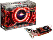
PowerColor launched the world's first single-slot + low-profile graphics card based on the Radeon HD 7750, the PowerColor HD 7750 LP. The card relies on a compact air-cooler, which uses a dense hive of aluminum fins, ventilated by a 40 mm lateral-flow fan to cool the 1.5 billion transistor GPU. The card draws power from the PCI-Express slot, and uses high-grade VRM components (such as CPL-made chokes, LFPAK MOSFETs, etc.,) to condition power at minimal board footprint.

The card doesn't compromise on clock speeds, and ships with 800 MHz GPU and 1125 MHz (4.50 GHz GDDR5 effective) memory clock speeds. Built on the 28 nm "Cape Verde" silicon, the Radeon HD 7750 packs 512 Graphics CoreNext stream processors, 32 TMUs, 16 ROPs, and a 128-bit wide GDDR5 memory interface, holding 1 GB of memory. The display connectors on PowerColor's card include one each of dual-link DVI, HDMI 1.4a, and D-Sub (detachable). The card's accessories include a low-profile bracket. PowerColor did not reveal pricing.

ASUS Readies ROG ARES 2 Graphics Card with Dual-HD 7870 GPUs

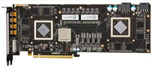
ASUS is working on its second Republic of Gamers (ROG) ARES graphics card, the ARES 2 dual-HD 7870. Its first ARES was dual-HD 5870. ASUS' decision to go with a pair of Radeon HD 7870 GPUs, instead of the premium HD 7970, certainly comes as a surprise. With it, one could deduce the target market-segment ASUS is aiming at: US $650-750, providing a solution that outperforms even the fastest HD 7970 GHz Edition and GTX 680 graphics cards, while being cheaper than Radeon HD 7990 (which is MIA), dual-HD 7970 X2, and of course, the GTX 690.

ASUS ARES 2 will back two 28 nm "Pitcairn" GPUs with all components unlocked; likely factory-overclocked speeds beyond those of the HD 7870 GHz Edition; and a total of 4 GB of GDDR5 memory (2 GB per GPU system). The card will draw power from two 8-pin PCIe power connectors, and will have a TDP of around 300W. It will take advantage of AMD ZeroCore CrossFire, with which it powers down the second GPU when not gaming, or with light 3D loads that the first GPU can munch on. With the monitor idling for a set amount of time, both GPUs power down. It's likely that ASUS will use a triple-slot cooling solution, despite the fact that the HD 7870 is a generally cool GPU. Pictured below is the first-generation ROG ARES (dual-HD 5870).

Update Jun 26: We have received word from ASUS that "There is no plan to release a dual 7870 VGA".

AMD Adopts 28 nm Bulk Manufacturing in 2013

According to AMD senior VP and CTO Mark Papermaster, the company will adopt the 28 nanometer bulk CMOS silicon fabrication process for its chips in 2013. The bulk process is used to manufacture high-volume and less-complex products, such as motherboard chipset, entry-level APUs, etc. The company already takes advantage of TSMC 28 nm High-Performance process for highly-complex chip designs, such as its Southern Islands GPU family, and will continue using it for its next-generation "Sea Islands" GPUs. In related news, DigiTimes learned through sources that AMD's Sea Islands GPUs have entered tape-out stage, and are on course for a late-2012 volume manufacturing, and early-2013 launch schedule.

Sapphire Squeezes Radeon HD 7750 Down to Single-Slot Low-Profile

What you might pass away for a bare entry-level graphics card at first glance, could end up being Sapphire's new Radeon HD 7750 single-slot low-profile graphics card. The design is a beneficiary of 28 nm "Cape Verde" silicon, which is found to have good-enough temperatures on its reference-design board. The card is ideal for mini-ITX systems. It relies entirely on the PCI-Express slot for power, and uses a 2+1+1 phase VRM, which utilizes high-grade driver-MOSFETs on its GPU phases.

The card sticks to AMD reference clock speeds of 800 MHz core, with 1125 MHz (4.50 GHz effective) memory. It packs 1 GB of GDDR5 memory over a 128-bit wide memory interface. The GPU packs 512 Graphics CoreNext stream processors. Display outputs include one each of dual-link DVI, mini-DisplayPort, and mini-HDMI. Adapters converting them to standard-size connectors, and a low-profile bracket will come included.

New Details on ASUS ZEUS Emerge

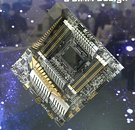
A star attraction at the motherboard section of ASUS booth was its ZEUS Dual-GPU X79 concept motherboard. We got a chance to talk at lengths with people at ASUS about the exhibit, and learned a few details beyond what we already know. To begin with, ASUS is likely using a pair of "Southern Islands" family discrete mobile GPUs, not desktop ones. Further, it's likely that the GPUs are 28 nm "Pitcairn" based. The two GPUs are installed in CrossFire configuration. The next big detail is that the design focus on [evidently] isn't the integrated dual-GPU, but to demonstrate the first Thunderbolt-equipped X79 motherboard. The ZEUS has not one, but two Thunderbolt ports. The third (and most depressing) detail is that it's "highly unlikely" that the ZEUS will ever make it to the market. Think of it as yet another tradeshow concept by a big company. Perhaps ASUS doesn't want the ZEUS to end up like the ROG GSurf-365, its first off-beat ROG motherboard, which went beyond the show-floor but didn't have market-success.

ASUS ROG MARS III Dual GTX 680 Graphics Card Detailed

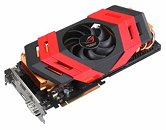
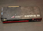
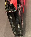
The ROG MATRIX 7970 wasn't the only new Republic of Gamers graphics card on display at Computex, it was sitting next to the MARS III. This monstrosity is a dual-GeForce GTX 680 graphics card, it packs two 28 nm GK104 GPUs with clock speeds that match or exceed those of the GeForce GTX 680. ASUS stopped short of revealing the clock speeds. The card draws power from three 8-pin PCI-Express power connectors, next to it is an instant fan-override button that revs up the card's fans to 100%. The card gives out three dual-link DVI display outputs, and is capable of driving 3D Vision Surround using three >1920x1200 pixels displays. Unlike the MATRIX 7970 and countless recent examples of ASUS' ugly fixation with triple-slot cooling solutions, it's a pleasant surprise seeing that the triple-fan cooling solution of the MARS III needs just two expansion card slots. The MARS III will be manufactured in limited quantities, and will probably cost more than a GeForce GTX 690.

GeForce GTX 680 A Sellout Success: NVIDIA

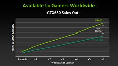
NVIDIA's flagship single-GPU graphics card, the GeForce GTX 680, achieved performance leadership over AMD's Radeon HD 7970, and forced a price-cut, however, a section of the community feels that availability is an issue with it. According to NVIDIA, availability is attributed to sales, and not lack of volumes. At an annual investors' meeting with the company's top-brass, NVIDIA released a slide which depicts GeForce GTX 680 as having 60% higher sales than GeForce GTX 580, six weeks following their respective launches.

There is one cosmetic inaccuracy in the graph, though. GeForce GTX 680 and GTX 580 are labeled "GT". One inference that can be drawn out of the graph is that NVIDIA is seeing some success in putting the 28 nm silicon fabrication process to use, despite the GTX 680 being one of the first chips built on it. In comparison, the GTX 580 arrived when the 40 nm process achieved a higher level of maturity. There seems to be a genuinely high demand for the GTX 680.

AMD AIB Partners Said to be Working on "HD 7970 X2"

Although AMD has plans to unveil its dual-GPU Radeon HD 7990 some time during Computex 2012, next month, it is reported that its add-in board (AIB) partners will be rolling out custom-design dual-GPU graphics cards labelled "Radeon HD 7970 X2." These cards most likely feature a pair of 28 nm "Tahiti" GPUs with high GPU clock speeds (perhaps above those of the HD 7990, perhaps even over 1 GHz). The new cards could then target the performance levels of NVIDIA's GeForce GTX 690 at competitive prices. It could also be AMD's strategy to give the onus to AIB partners to come up with "off-spec" dual-GPU cards to compete with GTX 690 in terms of performance, while maintaining an "on-spec" Radeon HD 7990 that seeks a higher price-performance ratio than that of the GTX 690.

ELSA Catches Up With Its Gladiac GeForce GTX 670 Graphics Card

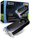
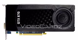
Japanese company ELSA, which specializes in Quadro and GeForce graphics cards, finally unveiled its Gladiac GeForce GTX 670 graphics card (model: GD670-2GERX). Pictured below, the ELSA's card sticks to NVIDIA reference design, except for the color of the PCB. It even sticks to reference clock speeds of 915 MHz core, 980 MHz GPU Boost, and 6008 MHz memory (GDDR5 effective). Based on the 28 nm GK104 silicon, the GTX 670 packs 1344 CUDA cores, a 256-bit wide GDDR5 memory interface, holding 2 GB of memory, on this card. It is priced at 52,800 JPY.

NVIDIA Readies GK104-based GeForce GTX 680M for Computex

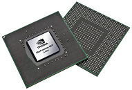
NVIDIA is readying a high-performance mobile GPU for a Computex 2012 unveiling. Called the GeForce GTX 680M, the chip is based on its trusty 28 nm GK104 silicon, but with about half its streaming multiprocessors disabled, resulting in a CUDA core count of around 768. Reference MXM boards of the chip could ship with memory options as high as 4 GB, across a 256-bit wide memory interface. With the right craftsmanship on the part of NVIDIA, the GTX 680M could end up with a power draw of 100W. A Chinese source had the opportunity to picture the reference board qualification sample, and put it through 3DMark 11, in which it was found to be roughly 37% faster than the GF114-based GeForce GTX 670M, scoring 4905 points in Performance preset. The test bed was driven by Intel Core i7-3720QM quad-core mobile processor.
HIS Readies Fanless Radeon HD 7750 iSilence 5 Graphics Card

HIS is ready with a fanless Radeon HD 7750 graphics card that utilizes the company's iSilence 5 cooling solution, which is used on the recently-launched HD 6670 iSilence 5. The cooler consists of a swanky-looking aluminum fin stack to which heat is conveyed by four 8 mm-thick nickel-plated copper heat pipes, which make direct contact with the GPU die. The heat is then passively dissipated by the aluminum fins.

The HIS Radeon HD 7750 iSilence 5 sticks to AMD reference clock speeds. The 28 nm "Cape Verde" GPU, in the HD 7750 configuration, packs 512 Graphics CoreNext stream processors, and a 128-bit wide GDDR5 memory interface, holding 1 GB of memory. The card relies on the PCI-Express slot entirely for its power. Display outputs include one each of dual-link DVI, HDMI, and DisplayPort. HIS is expected to unveil the card at Computex, after which, it joins the league of passive Radeon HD 7000 series graphics cards such as PowerColor HD 7750 Go Green and Sapphire HD 7750 Ultimate.

SPARKLE GeForce GTX 680 Inferno Unveiled

Sparkle, one of the leading manufacturers of graphics cards, revealed today its brand new GTX 680 Inferno, using NVIDIA's 28 nm Kepler GPU architecture and GPU Boost technology, which dynamically adjusts GPU speeds to maximize gaming performance up to 2 times higher than GTX 580. SPARKLE GTX 680 Inferno brings you a most fantastic gaming experience to satisfy all hardcore PC gamers' requirements.

Kepler architecture makes a giant leap in efficient-performance
Featuring 1536 CUDA cores, 1006 MHz GPU clock and 2GB of high-speed GDDR5 memory,

SPARKLE's flagship 28 nm GTX 680 Inferno graphics card greatly improves system power consumption and supports the latest PCI Express Gen 3 standards. The card requires two 6-pin power connectors, as the card has a TDP of only 195W. SPARKLE GTX 680 Inferno is not only faster but also operates at a much lower temperature and consumes lesser power than its rivals.

TSMC Gives NVIDIA Priority for 28 nm Manufacturing

Relations between NVIDIA and its principal foundry partner, TSMC, have been unpredictable in recent times, with reports of NVIDIA expressing displeasure with it over 28 nm manufacturing capacity, which is denting its competitiveness; and later crediting collaboration with it, for the energy-efficiency of its latest Kepler family of GPUs. With NVIDIA threatening to find other foundry partners for bulk manufacturing, and reports of Samsung already preparing qualification samples for it, TSMC is responding by issuing NVIDIA a priority over other clients (such as Qualcomm, AMD) for manufacturing of 28 nm chips.

While being unsatisfied with TSMC's output, and its new policy of charging for wafers rather than working chips yielded, NVIDIA refuted rumors of it seeking other foundry partners such as Samsung and Global Foundries. When put on high-priority, TSMC will facilitate speedy launch of new NVIDIA GeForce SKUs towards the end of Q2, 2012. Supply prioritization isn't new, TSMC has, in the past, prioritized Qualcomm when it threatened to shift allocations to other foundries. It remains to be seen how AMD responds to the situation, as such a prioritization would come at the expense of its volumes, and could threaten its competitiveness.

NVIDIA's GeForce GTX 670 Short PCB Pictured Up Close

Thanks to the impressive power-draw and temperature figures its GeForce GTX 680 could come up with, NVIDIA's newest SKU based on the 28 nm GK104 silicon, the GeForce GTX 670, will feature a compact PCB. The reverse side of this PCB was first pictured on a Colorful-branded graphics card. A picture of its obverse side was posted earlier today. In comparison to the GTX 680, the GTX 670 PCB is quite short. The eight GDDR5 memory chips are distributed between both the sides, these chips are wired to the GPU over a 256-bit wide memory interface. The VRM area is pushed towards the front-end of the PCB. It consists of a 4+2 phase design. The card draws power from two 6-pin PCIe power connectors. Display outputs include two dual-link DVI, and one each of HDMI and DisplayPort. There are two SLI bridge connectors, giving it 4-way SLI capability.

NVIDIA GeForce GTX 690 Starts Selling

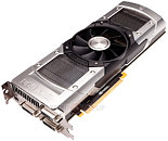
Announced last week, NVIDIA GeForce GTX 690 enthusiast graphics card started selling, at an MSRP of US $999 (prices vary greatly by region). A variety of add-in card (AIC) partners will launch their GTX 690 graphics cards today. The GeForce GTX 690 is a dual-GPU graphics card that packs two 28 nm GeForce Kepler 104 GPUs, arranged in an internal SLI configuration. Both these chips have all their components unlocked, including 1536 CUDA cores, and 2 GB of GDDR5 memory across a 256-bit wide memory interface. The card hence ends up with a total of 3072 CUDA cores, and 4 GB of memory. The card should be available on leading retail stores. Despite its high price, it could sell out fast.

TSMC's 28 nm Based ARM Cortex-A9 Test Chip Reaches Beyond 3 GHz

TSMC today announced its 28 nm high performance ARM Cortex-A9 dual-core processor test chip achieved 3.1 GHz performance under typical conditions.

The TSMC 28 nm HPM (high performance for mobile applications) process technology that achieved these results addresses applications requiring both high speed and low leakage power. Using various design signoff conditions, ARM A9 at TSMC 28HPM delivers performance speed range from 1.5 GHz to 2.0 GHz, suitable for mobile computing, and up to 3.1 GHz for high-performance uses. With its wide performance-to-leakage coverage, the 28 nm HPM process was developed for devices targeting networking, tablet and mobile consumer product applications.

Third GK104-based Single GPU Graphics Card SKU Detailed

After GeForce GTX 680, which has all components of the 28 nm GK104 enabled, a dual-GPU GeForce GTX 690, which features two of these chips, and the GeForce GTX 670, NVIDIA is readying its third single-GPU GK104-based SKU. We know from older reports that this SKU could be named GeForce GTX 660 (Ti). A fresh report suggests that it will be carved out by disabling an entire graphics processing cluster (GPC) on the GK104 silicon, resulting in a CUDA core count of 1152; reducing the memory bus width of 192-bit GDDR5; and most likely reducing the ROP count to 24. This SKU could be used to capture a price point of around US $249, targeting AMD's Radeon HD 7800 series.

Reference NVIDIA GeForce GTX 670 Graphics Card Pictured

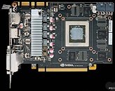
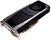
Here is the first picture of an NVIDIA reference design GeForce GTX 670. For the most part, its design will resemble that of reference design GTX 680. The card pictured below is said to have had Leadtek branding, which later got removed. GeForce GTX 670 is carved out of 28 nm GK104 silicon by disabling one of the card's eight SMX units, resulting in a CUDA core count of 1344. Its clock speeds are lower than those of the GTX 680, with around 950 MHz core base clock, and core boost clock a little over 1 GHz. It features 2 GB of memory across a 256-bit wide GDDR5 memory interface. The latest price speculation puts it at US $399-$429.

NVIDIA Credits Close Collaboration with TSMC for Kepler's Energy Efficiency

Despite the fact that NVIDIA is frantically seeking out other semiconductor foundries for high-volume manufacturing its 28 nm chip designs, and despite some looming irritants, NVIDIA appears to value its relationship with TSMC highly. NVIDIA's senior vice president for Advanced Technology Group Joe Greco, in a recent company blog post, credited close collaboration with TSMC for the stellar energy-efficiency (performance/Watt) figures NVIDIA's Kepler architecture has been able to achieve.

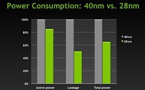
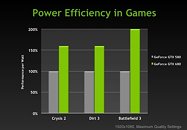
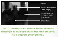
"The advancement that TSMC offered was a new optimized process technology. Kepler is manufactured using TSMC's 28nm high performance (HP) process, the foundry's most advanced 28nm process which uses their first-generation high-K metal gate (HKMG) technology and second generation SiGe (Silicon Germanium) straining," read the blog post. "Using TSMC's 28nm HP process enabled us to reduce active power by about 15 percent and leakage by about 50 percent compared to 40nm, resulting in an overall improvement in power efficiency of about 35 percent (see charts)."

Club 3D Releases Radeon HD 7870 JokerCard Graphics Card

Club 3D proudly presents the Club 3D Radeon HD 7870 jokerCard graphics card. With PokerSeries Club 3D offers a new level of special gamecards that delivers the best performance, newest features and best coolers. The jokerCard present our highest demands. Get ready for the future with 28 nm GPU technology, Graphics Core Next Architecture, AMD App Acceleration and support for Ultra HD 4096p resolutions and PCI Express 3.0.

If you expect above average performance of your Graphics card, Club 3D CoolStream High Performance Cooling Technology is just the kind of high performance that you have been looking for. Club 3D CoolStream features high performance heatpipes that keeps the components cool and outperforms standard cooling solutions. Transferring heat from the center area to each fin, ensuring enhanced heat dissipipation. The result is a dramatic increase of performance for your gaming and multimedia experience.

NVIDIA Releases GK107-based GT 630, GT 645 and 3 GT 640 Variants to OEMs

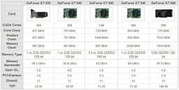
NVIDIA released its first desktop graphics cards based on its 28 nm GK107 silicon, in as many as three models, the GeForce GT 630, GT 640, GT 640 (second variant). Apart from these, NVIDIA appears to have launched two more models, one labeled GT 640, and another GT 645, which are based on previous generation GF116 and GF114, respectively. These new SKUs are available only to OEM partners, who will implement them in their new desktop PC designs.

Of the five new SKUs, the GT 630 and GT 640 (28 nm) are most interesting, as they are based on the GK107 silicon, with as many as 384 CUDA cores, and TDP as low as 50W. The GT 630 is a single-slot, low-profile graphics card with 384 CUDA cores, and a 128-bit wide GDDR5 memory interface, 875 MHz GPU clock speed, and 891 MHz memory clock speed. The GT 640 (28 nm) features different clock speeds. The specifications may seem confusing to the end user, but then they really don't concern people who buy retail-channel graphics cards. NVIDIA and AMD design OEM-specific SKUs completely à la carte, to OEM partners' requirements.

NVIDIA Licenses Integrated, OV-Tolerant I/O and ESD Tech. from Sofics and ICsense

Sofics bvba of Gistel, a leading provider of ESD solutions for ICs, and ICsense of Leuven, a prominent designer of analog, mixed-signal, and high-voltage ICs and turnkey ASICs, today announced that NVIDIA has licensed their integrated ESD and I/O technology to provide a stable 3.3V I/O with robust ESD protection on its Icera modem processors that use 1.8V transistors.

The license includes customized ESD solutions from Sofics and ICsense's overvoltage-tolerant I/Os. These solutions are based on a novel circuit technique proven in TSMC 0.18 um, 40 nm, and 28 nm processes that allows I/Os to handle more than 2X the voltage of the transistors on the chip.

AMD Chooses Computex 2012 as Radeon HD 7990 Launchpad

Even as NVIDIA is on the verge of unveiling its GeForce GTX 690 dual-GPU graphics card, at GeForce LAN Shanghai, AMD is in no hurry. Its competitive graphics card to the GTX 690, the Radeon HD 7990 "New Zealand", will be kept under the wraps till Computex 2012 (early June), DonanimHaber learned. Radeon HD 7990 will pack two completely unlocked 28 nm "Tahiti" GPUs, a total of 4,096 Graphics CoreNext stream processors, 6 GB of GDDR5 memory, and the ability to drive 6-monitor Eyefinity, out of the box.

NVIDIA Wants 450 mm Wafers, Seeking Foundry Partnership with GlobalFoundries, Samsung

NVIDIA is formulating a long-term chip manufacturing strategy that will see its interests secure by the time chip manufacturing has moved on to 14 nm (which follows 20 nm and today's 28 nm), which could arrive around 2015. Chip manufacturing by foundry partners is a potentially major irritant for NVIDIA, which wants to see wafer sizes getting increased from the current 300 mm manufacturing at TSMC, to 450 mm, and fast. TSMC will achieve 450 mm (18-inch) wafer manufacturing capability only by 2015. Another irritant for NVIDIA is TSMC's change in business model, which charges fabless customers "per wafer manufactured", rather than "per working chip yielded", giving them what they perceive to be the shorter end of the stick. NVIDIA is thus rigorously evaluating other foundry partners. We know from a slightly older report that Samsung has sent NVIDIA test chips manufactured at its Austin, Texas facility. There is talk that NVIDIA could also seek partnerships with GlobalFoundries, of which AMD recently relinquished all its stakes on. NVIDIA needs reliable, high-volume foundry partners that can keep it competitive not just with its main business of GPUs, but also a potential gold mine that is application processors.

AMD Radeon HD 7970M Arrives on 24th

The next "AMD Tuesday" is the coming one, on which the company plans to launch Radeon HD 7970M, its next high-end discrete GPU for notebooks. Codenamed "Thames", the HD 7970M will be based on the 28 nm "Pitcairn" silicon, on which desktop Radeon HD 7800 series, is also based. When launched, the HD 7970M could become the fastest notebook discrete GPU, since NVIDIA's fastest discrete notebook GPU, and the GeForce GTX 675M are based on previous-generation 40 nm GF114, over which Pitcairn already established a performance lead, in the desktop front. We are hearing that notebook vendors already have their designs based on this chip ready in the pipeline.
Return to Keyword Browsing
Nov 23rd, 2024 07:42 EST change timezone

New Forum Posts

Popular Reviews

Controversial News Posts