News Posts matching #40 nm

Return to Keyword Browsing

Radeon HD 5870 Aggressively Priced: Report

According to a fresh report by Donanim Haber, AMD's next performance graphics accelerator, the Radeon HD 5870, codenamed "Cypress" is expected to be aggressively priced, at US $299. At that price, it intends to be highly competitive against GeForce GTX 285 from NVIDIA. The secret-sauce behind the price could be the 40 nm fab process on which the GPU is being built, which allows upping transistor counts while maintaining significantly smaller die-sizes compared to 55 nm.

There is a great deal of uncertainty surrounding the specifications of the GPU, including what level of performance with existing application could it end up offering. Some sources, such as ChipHell, which are one of the first to leak pictures of components related to various Evergreen family products claim the Cypress GPU to have an almost 100% increase in stream processor counts compared to RV770, while others remain conservative expecting it to be around 50%. With this kind of a pricing, Cypress could trigger market-wide changes in GPU pricing, if it ends up with a good price/performance ratio at $299.

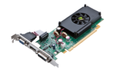
NVIDIA GeForce G210 and GeForce GT 220 Now Official

Earlier this week we informed you of the existance of two upcoming 40 nm NVIDIA parts, GeForce GT 220 and GeForce G210. We also gave a hypothetical release date which stated "early Q4", well we lied to you in a good way, the cards are already official and standing on NVIDIA's official page.
Both cards support DirectX 10.1, OpenGL 3.0 and CUDA, with the G210 having analog VGA, DisplayPort and DVI outputs while the GT 220 has VGA, HDMI and DVI. The GeForce G210 has 16 processor cores and a 589 MHz CPU clock speed; that's paired with 512 MB of DDR2 memory with a 64-bit interface and 500 MHz clock speed. Its shaders run at 1402 MHz. As for the NVIDIA GeForce GT 220, it has 48 processor cores and a 615 MHz clock speed, paired with 1 GB of GDDR3 memory with a 790 MHz clock and a 128-bit interface. It has a slightly slower shaders clock speed of 1335 MHz. Neither of the two cards is expected to be available directly to consumers, both offerings are marked as OEM products and meant to be entry-level options in pre-built PCs.

NVIDIA GeForce G210 (OEM Product) Specs
NVIDIA GeForce GT 220 (OEM Product) Specs

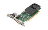
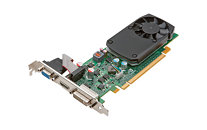
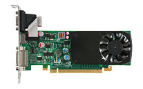
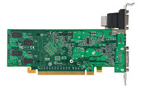
GeForce GT 220, G 210 Reference Designs Pictured

NVIDIA's upcoming 40 nm value GPUs, GeForce GT 220 and GeForce G 210 are on their way to a early Q4 launch. NVIDIA looks to give its 40 nm desktop GPUs the right profile with its reference designs that include low-profile (half-height), single-slot PCBs and coolers. The size and shape of these cards send out good signals about their thermal characteristics, at least for now.

Both these cards use essentially similar designs: a half-height PCB holds the GPU one one end, and memory chips are distributed on the front and back sides of the PCB. The G 210 offers DVI-D and DisplayPort connectors on the card, while the GT 220 offers DVI-D and HDMI. Both cards feature extensions for the D-Sub connector. The GT 220 has a slightly longer PCB, with a dense aluminum cooler. Both cards rely entirely on the PCI-Express slot for power. G 210 features 24 shaders, 512 MB of 64-bit DDR2 or GDDR3 memory, while the GT 220 features 48 shaders, up to 1 GB of 128-bit GDDR3 memory. Pictured below are GT 220 and G 210 and angled, front, and back pictures in the said order.

GeForce G 210 and GT 220 Surface

DirectX 11 isn't far from its being an official industrial standard. Both NVIDIA and AMD have high-end graphics processors supporting the standard in the works, though it is expected that by the time DirectX 11 reaches the masses, we will be into 2010. On the course, both companies have the time to perfect their designs on the new 40 nm silicon fabrication technology, which will build the first waves of DirectX 11 GPUs. One of the best ways of doing this is by building products based on the current architecture on the new process, and testing the foundry-companies' abilities to handle large market demands, while benefiting from low-manufacturing costs. Following AMD's introduction of the RV740, NVIDIA recently announced a new class of mGPUs based on the 40 nm process, and is having concrete plans of selling their desktop versions by this October.

Two of the important starting points for NVIDIA are the GT218 and GT216 graphics processors. The two have already being assigned mGPU branding of GeForce G 210M and GeForce GT 230M respectively. Their desktop versions are to be branded GeForce G 210 and GeForce GT 220 respectively. VR-Zone sourced the specifications of these GPUs, by running them on the upcoming GeForce 190.15 drivers.

AMD Radeon RV840 Graphics Card Caught on Camera

Yesterday, AMD unveiled its surprise for this year's Computex, with a demonstration of a DirectX 11 3D scene. Behind the scenes though, was what AMD claimed to be the "world's first true DirectX 11 graphics processor". The hardware itself however, wasn't publicly displayed, although a memento of AMD's partnership with TSMC, a wafer of 40 nm DirectX 11 GPUs, was made public. VR-Zone however, sneaked into the backdrops and pictured the machine that ran the demo (which ironically, was built into a case with a side-window).

The graphics card, a portion of which, is hidden behind the "wing" of the AMD Dragon logo graphic, is seen to be about 8.5 inches long, spans across two slots, and has a seemingly sporty cooler with the ATI-red shroud. It draws power from a single 6-pin PCI-E connector. The photographers note that this could be the RV840-based desktop accelerator, which forms the performance-mainstream product for the company's upcoming DirectX 11-compliant GPU lineup codenamed "Evergreen". The first product from this series is expected to be released in September, weeks ahead of the launch of Microsoft Windows 7.

AMD to Cut HD 4850 Prices to Compensate for HD 4770 Shortages

It seems that in order to make up for the shortages of the now very popular HD 4770, due to TSMC's issues with 40 nm manufacturing, AMD is dropping the prices of the HD 4850 to around the MSRP of the HD 4770. That is around $99.99 US and about €90, this will be putting further pressure on NVIDIA as AMD brings down one of its top GPUs in to the sub-$100 market.

At Least 30% of NVIDIA GPU Shipments on TSMC 40 nm Process by End of 2009

Nearly a month since AMD's introduction of the 40 nm RV740 GPU, there is still no concrete sign of a 40 nm GPU from NVIDIA slated for anytime soon, apart from timely scoops on the GT300. Sources at graphics card vendors however seem confident that by the end of 2009, 40 nm GPUs will constitute at least 30% of NVIDIA's GPU shipments, that too sourced from TSMC, a foundry-partner which has been in the news off late, for technical problems with their 40 nm node, that are affecting its output efficiency.

What's more, NVIDIA seems to have expressed interest in becoming one of the first clients for TSMC's upcoming 28 nm process that is expected to become a reality in Q1 2010. This should also tell you that for GPUs, the next step for silicon fabrication technology will be 28 nm, unlike 32 nm for CPUs.

NVIDIA GT300 Already Taped Out

NVIDIA's upcoming next-generation graphics processor, codenamed GT300 is on course for launch later this year. Its development seems to have crossed an important milestone, with news emerging that the company has already taped out some of the first engineering samples of the GPU, under the A1 batch. The development of the GPU is significant since it is the first high-end GPU to be designed on the 40 nm silicon process. Both NVIDIA and AMD however, are facing issues with the 40 nm manufacturing node of TSMC, the principal foundry-partner for the two. Due to this reason, the chip might be built by another foundry partner (yet to be known) the two are reaching out to. UMC could be a possibility, as it has recently announced its 40 nm node that is ready for "real, high-performance" designs.

The GT300 comes in three basic forms, which perhaps are differentiated by batch quality processing: G300 (that make it to consumer graphics, GeForce series), GT300 (that make it to high-performance computing products, Tesla series), and G200GL (that make it to professional/enterprise graphics, Quadro series). From what we know so far, the core features 512 shader processors, a revamped data processing model in the form of MIMD, and will feature a 512-bit wide GDDR5 memory interface to churn out around 256 GB/s of memory bandwidth. The GPU is compliant with DirectX 11, which makes its entry with Microsoft Windows 7 later this year, and can be found in release candidate versions of the OS already.

Radeon HD 4770 Released, Industry's First 40 nm GPU

AMD today released the ATI Radeon HD 4770 graphics card. The release marks several milestones for the company, mainly winning the race for the first GPU to be built on the 40 nm process, and the introduction second-generation GDDR5 memory for the mainstream consumer segment.

The brains of this card is the 40 nm AMD RV740 GPU. Its specifications include 640 stream processors that churn out over 900 GFLOPs of shader compute power, 32 texture memory units, and 16 render back-ends. The GPU is aided by 512 MB of fast GDDR5 memory across a 128-bit wide interface. This provides the same amount of bandwidth as 256-bit GDDR3 commonly found in most graphics card in the range. The card is DirectX 10.1 compliant, and supports the ATI CrossFireX multi-GPU standard.

The card has been launched worldwide, with its initial US price set at $109, and an optional rebate that can send its price further down. In its range, it competes with NVIDIA GeForce 9800 GT, and AMD's own Radeon HD 4830. TechPowerUp is one of the first technology portals to publish a thorough review of the Radeon HD 4770. Our review can be read here.

GT300 to Pack 512 Shader Processors

A real monster seems to be taking shape at NVIDIA. The company's next big graphics processor looks like a leap ahead of anything current-generation, the way G80 was when it released. It is already learned that the GPU will use a new MIMD (multiple instructions multiple data) mechanism for its highly parallel computing, which will be physically handled by not 384, but 512 shader processors. The count is a 112.5% increase over that of the existing GT200, which has 240.

NVIDIA has reportedly upped the SP count per cluster to 32, against 24 for the current architecture, and a cluster count of 16 (16 x 32 = 512). Also in place, will be 8 texture memory units (TMUs) per cluster, so 128 in all. What exactly makes the GT300 a leap is not only the fact that there is a serious increase in parallelism, but also an elementary change in the way a shader processor handles data and instructions, in theory, a more efficient way of doing it with MIMD. The new GPU will be DirectX 11 compliant, and be built on the 40 nm manufacturing process. We are yet to learn more about its memory subsystem. The GPU is expected to be released in Q4 2009.

NVIDIA Outsources 40 nm to Foundry Partners in Q2

With rival AMD having a production-grade 40 nm graphics processor, and UMC's recent announcement of being ready with a high-performance 40 nm manufacturing node, the conditions are increasingly favourable for NVIDIA to flag-off large-scale production of 40 nm GPUs. According to Chinese print-media Commercial Times, the company set its foundry outsourcing schedule for within Q2 2009, with TSMC and UMC being the regular foundry-partners.

Within this quarter, NVIDIA will start mass-production of the entry-level GT218, high-end mobile GT215 and mainstream desktop GT214 and GT216 GPUs. Additionally, the company may also expand its output for the 55 nm G200b high-end GPU.
Return to Keyword Browsing
Apr 18th, 2025 19:38 EDT change timezone

New Forum Posts

Popular Reviews

Controversial News Posts